Compact broadband inverse design of a 3 dB optical power splitter based on PSO in silicon photonics
Thuy Tran Thi Thanh1*
Tan Hung Nguyen2
Dung Truong Cao1
- Faculty of Electronics Engineering 1 & EDA Lab, Posts and Telecommunications Institute of Technology, Hanoi, Vietnam
- Advanced Institute of Science and Technology – The University of Danang, Danang, Vietnam
Article Info
Received 26 Feb. 2026
Received in revised form 25 Mar. 2026
Accepted 30 Mar. 2026
Available on-line 29 May 2026
Keywords: inverse design; PSO; silicon-on-insulator; FDTD; high performance. compact photonic components.
Abstract
Inverse design has emerged as a powerful approach for developing high-performance photonic devices beyond the limitations of conventional geometry-based methods. In this study, we propose a compact 3 dB optical power splitter designed using a boundary-based inverse design strategy driven by the particle swarm optimisation (PSO) algorithm. The device boundary along the propagation direction is discretised into fine segments and iteratively optimised through a two-stage framework to simultaneously suppress input reflection and achieve balanced power distribution at the output ports. Over a 100 nm bandwidth, the improved structure exhibits outstanding optical performance. The excess loss stays between −0.1 and −1.1 dB, but the reflection is decreased to about −20 dB. Nearly equal power splitting is seen at the middle wavelength when the balancing factor is close to 0 dB. The device also exhibits symmetric and consistent responses when excited from either input port. With a compact footprint of approximately 6 µm × 16 µm, the proposed design is suitable for high-density photonic integrated circuits. These results confirm the effectiveness of a PSO-based boundary inverse design for realising broadband, low-loss, and
1. Introduction
In the era of the fourth industrial revolution, the rapid growth of artificial intelligence, big data, cloud computing, and the internet of things (IoTs) has created an urgent demand for high-speed communication systems with ultralarge bandwidth and parallel processing capabilities [1–4]. Optical networks have emerged as a core solution due to their low propagation loss, ultra-high-data rates, and scalability. Optical signal processing performed directly in the optical domain eliminates optical–electrical conversions, enabling ultra-wide bandwidth, low loss, and high integration density [5–7].
The development of photonic integrated circuits (PICs) enables the integration of multiple optical functionalities onto a single chip, thereby reducing system size, lowering power consumption, and enhancing reliability. Within integrated photonic devices, key components such as multiplexers/demultiplexers, optical switches, modulators, and particularly optical power splitters play fundamental roles in distributing and controlling optical signals in interferometric structures, routing networks, and multiplexing systems. The optical power splitter not only directly affects transmission performance but also determines the insertion loss and power balance of the overall system. Currently, the silicon-on-insulator (SOI) platform is considered an optimal choice for fabricating photonic devices due to its high refractive index contrast, capability for high-density integration, and, most importantly, compatibility with CMOS technology. This compatibility enables large-scale, cost-effective manufacturing and seamless integration with electronic circuits, opening broad prospects for next-generation high-speed optical communication systems [8].
From a methodological perspective, the design of photonic devices is currently based on two principal approaches: forward or conventional design and inverse design. The conventional approach relies on the theoretical analysis of specific geometric structures, such as directional couplers [9], multimode interferometers (MMIs) [10, 11], and Y-junctions [12], to determine the corresponding optical transmission characteristics based on fundamental physical principles including reflection, interference, and mode coupling. This approach typically provides stable and controllable performance. However, due to its strong dependence on the designer’s experience, intuition, and approximate analytical models, the resulting device dimensions are often relatively large, thereby limiting the achievable integration density of silicon-based photonic devices [13, 14]. In contrast, the inverse design approach begins with predefined target specifications, such as transmission spectra, electromagnetic field distributions, power splitting ratios, or operational bandwidth, and subsequently employs optimisation algorithms to search for the optimal geometric configuration within a highdimensional parameter space to satisfy these objectives. By not being constrained to traditional structural templates and allowing the exploration of free-form geometries or pixelated topologies, inverse design significantly reduces device footprint while simultaneously enhancing performance and integration density. Consequently, this methodology opens new opportunities for the development of next-generation photonic integrated circuits.
In the inverse design of photonic devices, two widely adopted approaches are pixel-based representation and boundary-based (free-form) representation. In the pixelbased method, the design region is discretised into many small elements (pixels) with variable permittivity values, allowing the optimisation algorithm to freely distribute materials within the domain to achieve the desired objective. On the other hand, the boundary-based approach describes the device structure continuously parameterised interfaces, for example using spline functions or analytical expressions, thereby directly optimising the geometric shape of the device. This approach typically results in smoother structures and offers improved manufacturability in practical fabrication processes. To perform the optimisation procedure, various algorithms have been employed, including direct binary search (DBS) [15, 16], particle swarm optimisation (PSO), genetic algorithm (GA), the adjoint method (AM), as well as gradient-based optimisation techniques and artificial intelligence-driven approaches.
Many studies have employed pixel-based topology optimisation to achieve high-efficiency and broad bandwidth performance [15]. However, the resulting structures often exhibit irregular and non-smooth boundaries, which impose limitations on practical manufacturability. The DBS method has been applied to the design of compact 2 × 2 3 dB power splitters [15, 16]; nevertheless, it typically suffers from slow convergence and a tendency to become trapped in local minima when the number of design variables is large. Deep learning-based approaches, such as deep neural networks, have also been explored for the design of optical power splitters [17]. Despite their potential advantages, these methods strongly depend on the availability and quality of training data and are primarily focused on 1 × 2 configurations. Other works have demonstrated compact, broadband power splitters with experimental validation [18–20]; however, most of these designs still rely on discrete topology representations or emphasise dual-mode operation rather than true 2 × 2 structures with independent input ports. In addition, the work in [21] adopts a pixel-based inverse design approach rather than a simple parameter tuning of a conventional MMI. A smoothing procedure is incorporated to alleviate sharp boundaries in the discretised topology, and automatic differentiation (AD) is employed to efficiently compute gradients. Nevertheless, the design remains fundamentally based on a pixelated representation.
Existing studies predominantly adopt pixel-based representations or focus on 1 × 2 configurations. The design of a 2 × 2 optical power splitter based on a free-form boundary representation combined with a global optimisation algorithm such as PSO remains relatively unexplored, thereby presenting a promising research direction for achieving smooth geometries that are fabrication-friendly while maintaining high optical performance. In this paper, we propose the design and optimisation of a 2 × 2 optical power splitter using an inverse design methodology with a free-form boundary representation. The optimisation process is carried out using the PSO algorithm in conjunction with finite-difference time-domain (FDTD) simulations to maximise transmission efficiency, ensure balanced power splitting, and minimise insertion loss over a 100 nm bandwidth.
The remainder of this paper is organised as follows. Section 2 presents the inverse design methodology and the proposed device structure. Section 3 reports the simulation results and provides a detailed discussion. Finally, section 4 summarises the main conclusions of this research.
2. Inverse design methodology and device structure
In this paper, our objective is to design an optical power splitter with a 1:1 splitting ratio and an operating bandwidth of 100 nm using the fundamental mode. To achieve this objective, a PSO-based inverse design approach is employed to optimise the waveguide width within the design region. Specifically, the region is discretised along the propagation direction into many small segments, where the width of each segment is treated as an independent optimisation variable.
The initial structure and detailed design parameters represented in Fig. 1 and Table 1 have an input and output ports width of w = 0.45 µm, and the width and length of the design region are 6 µm. The structure is designed to work at the centre wavelength of 1.55 µm using the fundamental transverse electric (TE0) mode. The TE0 mode is a preferred choice in silicon photonic waveguides due to its numerous advantages. It is highly compatible with semiconductor diode lasers and offers a maximum modal momentum for optimal light confinement and exhibits minimal dispersion and loss. Furthermore, it maintains exceptional stability, demonstrating resilience to material imperfections. The core material of the proposed design is silicon (Si), with SiO2 as the cladding for oxide protection. The refractive indices of these two materials are approximately 3.5 for silicon and 1.45 for silicon dioxide. The proposed device can be fabricated using modern techniques, such as electron-beam writing or 193 nm deep ultraviolet (DUV) photolithography incorporated with dry etching, for example, inductively coupled plasma (ICP) etching.

Fig. 1. Initial structural diagram of a 3 dB optical power splitter.
Initial parameters of the proposed design.
| Parameter | Symbol | Value |
|---|---|---|
| Length of input/output | L | 5 µm |
| Width of input/output | w | 450 nm |
| Waveguide thickness (Si) | h | 220 nm |
| Refractive indices of the silicon core layer |
nr | 3.47 |
| Refractive indices of the cladding oxide layer |
nc | 1.444 |
| Width of design region | Wdes | 6 µm |
| Length of design region | Ldes | 6 µm |
| Length of gap | Gap | 1.55 µm |
To inversely design a 2 × 2 optical power splitter with two input ports and two output ports in such a way that the transmitted power is maximised, the splitting ratio approaches 1:1, and back-reflection is minimised, we propose a two-stage optimisation strategy employing two different figure of merit (FOM) functions, as illustrated in Fig. 2. Separating the problem into two independent objectives enables a better control of the physical characteristics of the device and improves the convergence behaviour of the optimisation algorithm in a highdimensional design space. The two stages are executed sequentially. At the beginning of the optimisation process, all design parameters are randomly initialised within predefined physical and fabrication constraints. In the first stage, the algorithm searches for an optimal solution that primarily suppresses back-reflection. Once the first stage converges or reaches the predefined stopping criterion, the optimised parameter set obtained at the end of Stage1 is directly used as the initial condition for Stage2. In the second stage, the parameters are further refined to enhance transmission efficiency and enforce a balanced 1:1 power splitting ratio between the two output ports. This sequential optimisation strategy ensures that the structure first achieves low reflection before being fine-tuned for balanced power distribution, thereby improving stability and overall convergence performance.
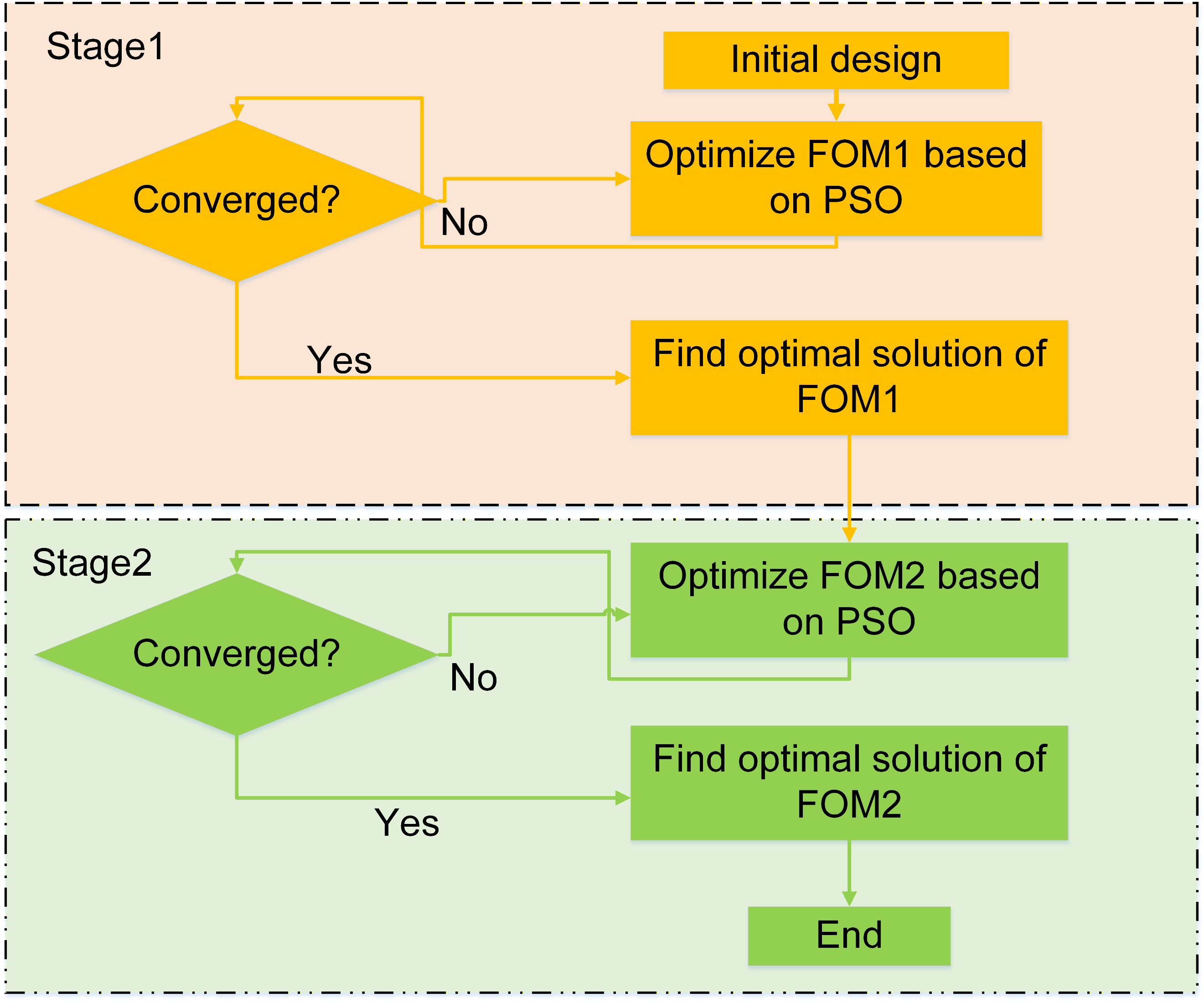
Fig. 2. Flowchart of inverse design based on PSO.
In the first stage, the primary objective is to suppress back-reflection toward the undesired port. The corresponding FOM is defined as:
where P2 denotes the normalised optical power measured at Port2 (reflection or undesired port). Minimising FOM1 ensures that the reflected power is reduced to the lowest possible level, thereby improving transmission efficiency and reducing insertion loss due to backward coupling. After achieving sufficiently low reflection, the second stage focuses on maximising transmitted power and enforcing a balanced 1:1 power splitting ratio between the two output ports. The second FOM is defined as:
where P3 and P4 represent the normalised output powers at Port3 and Port4, respectively. When P3 ≈ P4 ≈ 0.5, the value of FOM2 approaches one, indicating an equal power splitting condition with high transmission efficiency.
The PSO method is employed in both phases to repeatedly search for the optimal width distribution in order to implement the previously defined two-stage optimisation framework. In the PSO-based inverse design procedure, the design region along the propagation direction is discretised into 100 uniform segments. Accordingly, the design vector is defined as W = [ W1, W2, … W100], where each variable represents the local waveguide width of a corresponding segment. The initial width of all segments is uniformly set to 6 µm as the starting configuration of the optimisation process. Each particle in the swarm represents a candidate width profile of the photonic device, where the particle position encodes the waveguide width at each of the 100 discretised segments. For a given particle, the corresponding device structure is constructed according to its width distribution and numerically simulated using the FDTD method. The simulated optical response is then substituted into the predefined FOM to evaluate the performance device. During the optimisation process, particle velocities and positions are iteratively updated according to the standard PSO updating rules, which consider both the particle personal best width profile (pbest) and the global best width profile (gbest) found by the swarm. After each update, the FOM associated with the new width distribution is recalculated. If the obtained FOM exceeds the particle previous best value, the personal best solution is updated accordingly. Similarly, the global best solution is updated whenever a superior FOM is identified within the swarm. The optimisation continues until a convergence criterion is satisfied or a predefined maximum number of iterations is reached, ultimately yielding an optimised waveguide width profile with improved optical performance. Figure 3 shows the electromagnetic field of the power splitter with initial parameters. The optimal results for power splitter design using PSO are analysed in the following section.
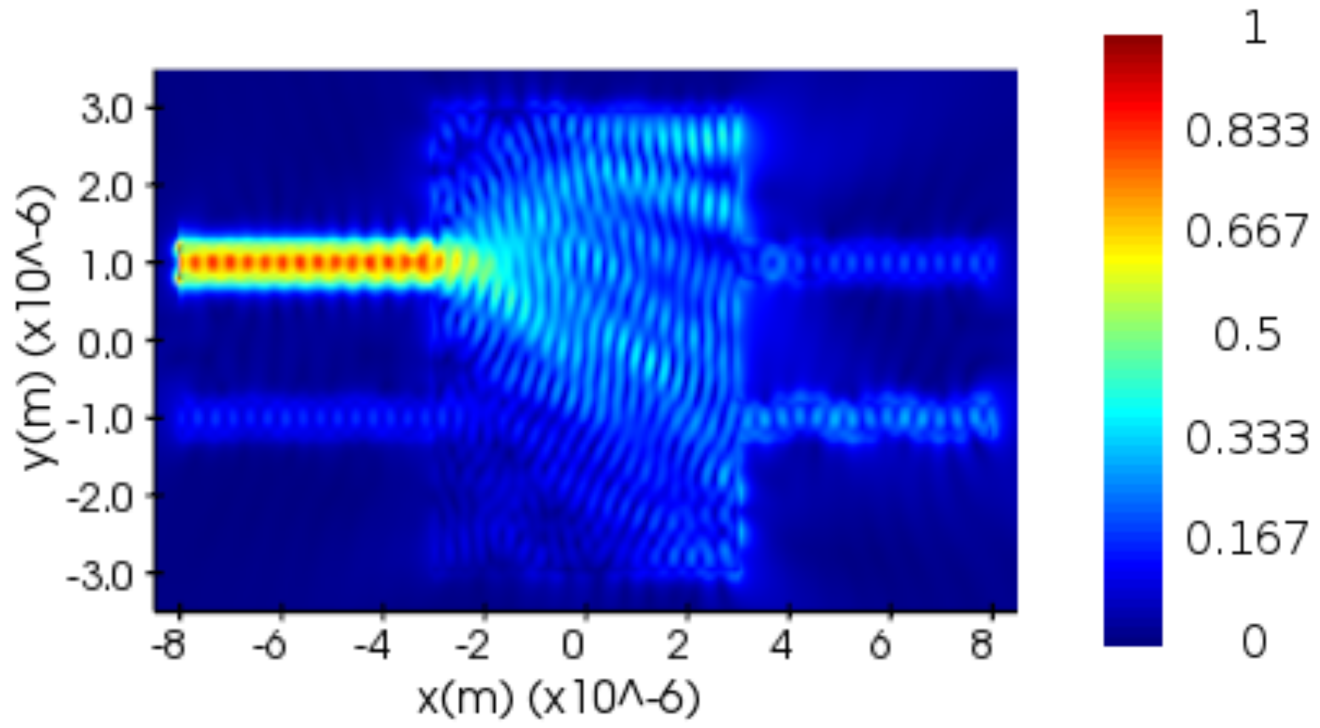
Fig. 3. The electromagnetic field of the initial device.
3. Simulation results and discussion
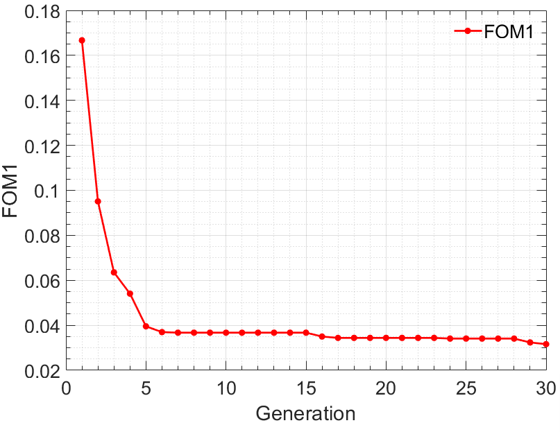
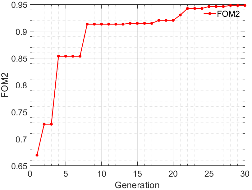
After establishing the inverse design framework based on the PSO algorithm, we performed the optimisation process in two sequential stages to simultaneously achieve low reflection loss and high power-splitting efficiency. Figure 4 illustrates the convergence behaviour of the two objective functions, FOM1 and FOM2, over 30 PSO generations, with Figure 4(a) showing the convergence of FOM1 and Figure 4(b) presenting the evolution of FOM2. In the first stage, FOM1 is defined to minimise the reflected power at the input port. The results show that FOM1 rapidly decreases to approximately 0.03, corresponding to a very low reflection. Notably, from the 5th generation onward, the convergence curve becomes nearly flat and reaches a saturation region, indicating that the algorithm quickly identifies a stable optimal solution with a strong convergence behaviour. In the second stage, FOM2 is formulated to maximise the total transmitted power at the two output ports while ensuring a 1:1 splitting ratio. The value of FOM2 gradually increases to approximately 0.95, approaching unity. This indicates that the transmitted power at the two output ports is high and nearly equally distributed. From around the 25th generation, the FOM2 curve also becomes saturated, demonstrating that the optimisation process has converged and the designed structure has reached a near-optimal state.
(a)
(b)
Fig. 4. The change of the (a) FOM1, (b) FOM2.
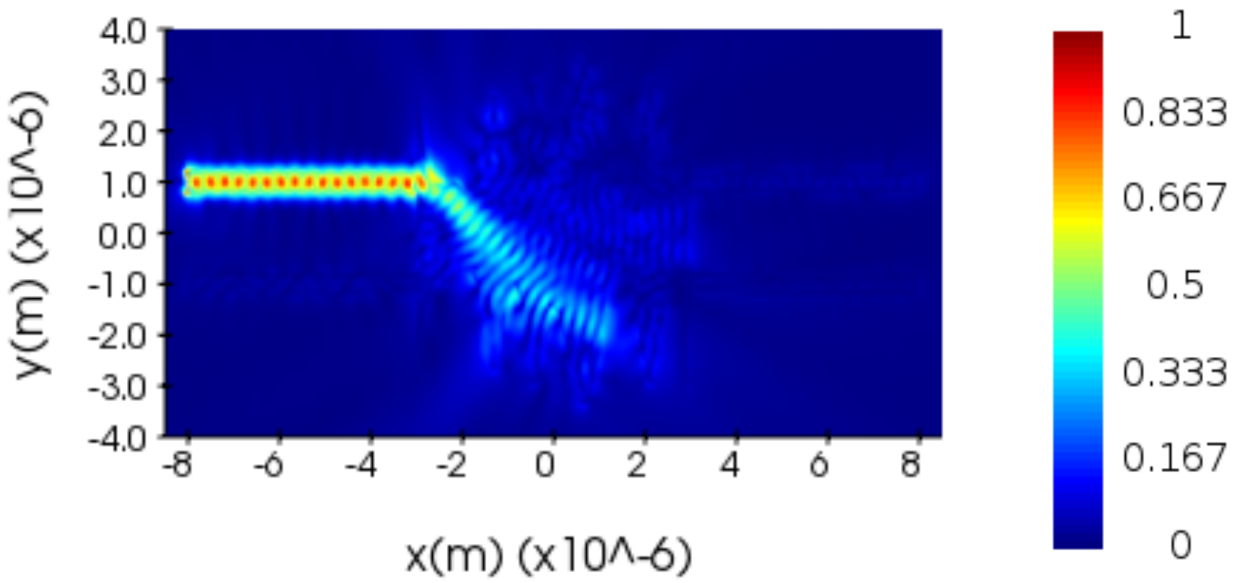
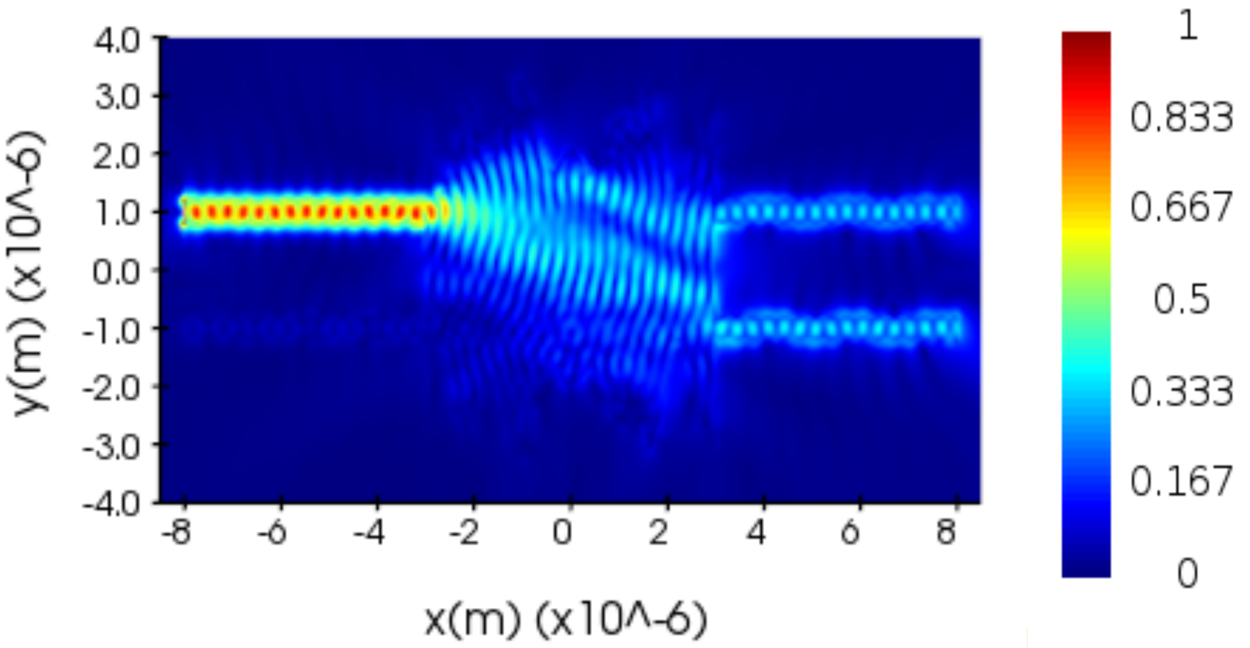
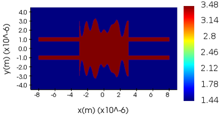
Figures 5(a) and 5(b) and Figures 6(a) and 6(b) present the electric field distribution and the optimised power splitter structure after the completion of the two optimisation stages, respectively. Figure 5 illustrates the steady and well-confined electric field propagation through the device, confirming low reflection and efficient power transmission. Figure 6 shows the final optimised geometry of the power splitter obtained after the two-stage PSO process where the width profile has been adjusted to achieve minimal reflection and nearly equal power distribution at the two output ports.
We also calculated the device excess loss (EL), balancing factor (BF), and reflection (R) across each port in order to benchmark its performance. These values may be found using the formula:

where P1 and P2 are the two normalised output powers, P3 and P4 are the two normalised input powers.
(a)
 `
`
(b)
Fig. 5. (a) Electromagnetic field distribution of the device at a wavelength of 1550 nm. (b) Optimised device structure after Stage1 (FOM1) at a wavelength of 1550 nm.
(a)
(b)
Fig. 6. (a) Electromagnetic field distribution of the device at a wavelength of 1550 nm. (b) Optimised device structure after Stage2 (FOM2) at a wavelength of 1550 nm.
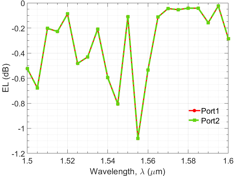
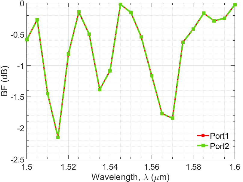
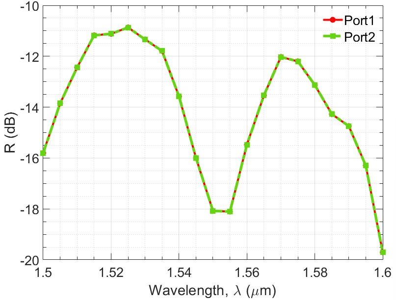
The performance metrics were further evaluated over the wavelength range of 1500–1600 nm, as illustrated in Fig. 7. The EL varies from approximately −0.1 dB to −1.1 dB across the considered bandwidth, indicating low insertion loss over a wide spectral range. The BF at the central wavelength approaches 0 dB, demonstrating nearly equal power splitting between the two output ports. Meanwhile, the R remains relatively low throughout the operating band and can reach values close to −20 dB, confirming effective suppression of back-reflected power and good impedance matching at the input port. Additionally, in Fig. 7, we also evaluate the device performance when light is launched from both input ports (Port1 and Port2). The results show nearly identical spectral responses in both cases, indicating symmetric structural behaviour and confirming that the optimised power splitter operates consistently regardless of the excitation port.
(a)
(b)
(c)
Fig. 7. Performance metrics as a function of wavelength: (a) excess loss (EL); (b) balancing factor (BF); (c) reflection (R).
After the performance evaluation, the optimised design corresponding to Fig. 6(b) can be exported in a GDS format for fabrication. The exported layout has a compact footprint of approximately 6 µm × 16 µm, making it suitable for integration in high-density photonic integrated circuits.
4. Conclusions
In conclusion, we propose the design of an optical power splitter using a boundary-based inverse design approach driven by the PSO algorithm. Instead of relying on conventional geometry-constrained structures, the device boundary is directly optimised to achieve low reflection and high transmission efficiency through a two-stage optimisation strategy. The optimised structure exhibits low reflection approaching −20 dB, EL ranging from −0.1 dB to −1.1 dB, and a balancing factor close to 0 dB at the central wavelength, indicating nearly equal power splitting. Broadband analysis over the 1500–1600 nm wavelength range confirms stable and consistent performance. In addition, symmetric operation is verified by exciting both input ports, yielding nearly identical spectral responses. Notably, the proposed device maintains a compact footprint of approximately 6 µm × 16 µm, making it highly suitable for high-density photonic integrated circuits. These results demonstrate that the PSO-based boundary inverse design method provides an effective and flexible framework for developing compact, low loss, and broadband photonic components.
Acknowledgement
Thuy Tran Thi Thanh was funded by the Master, Ph.D. Scholarship Programme of Vingroup Innovation Foundation (VINIF), code VINIF.2025.TS70.
References
[1] Essiambre, R. J., Foschini, G. J., Winzer, P. J., Kramer, G. & Goebel, B. Capacity limits of optical fiber networks. J. Light. Technol. 28, 662–701 (2010). - https://doi.org/10.1109/JLT.2009.2039464
[2] Guo, P. et al. WDM-MDM Silicon-Based Optical Switching for Data Center Networks. in ICC 2019 – 2019 IEEE International Conference on Communications 1–6 (IEEE, 2019). https://doi.org/10.1109/ICC.2019.8762082
[3] Lu, P., Zhang, L., Liu, X., Yao, J. & Zhu, Z. Highly efficient data migration and backup for big data applications in elastic optical inter-data-center networks. IEEE Netw. 29, 36–42 (2015). https://doi.org/10.1109/MNET.2015.7293303
[4] Gu, M., Li, X. & Cao, Y. Optical storage arrays: A perspective for future big data storage. Light Sci. Appl. 3, e177 (2014). https://doi.org/10.1038/lsa.2014.58
[5] Wang, J. & Long, Y. On-chip silicon photonic signaling and processing: A review. Sci. Bull. 63, 1267–1310 (2018). https://doi.org/10.1016/j.scib.2018.05.038
[6] Shekhar, S. et al. Roadmapping the next generation of silicon photonics. Nat. Commun. 15, 751 (2024). https://doi.org/10.1038/s41467-024-44750-0
[7] Asakawa, K., Sugimoto, Y. & Nakamura, S. Silicon photonics for telecom and data-com applications. Opto-Electron. Adv. 3, 200011 (2020). https://doi.org/10.29026/oea.2020.200011
[8] Izhaky, N. et al. Development of CMOS-compatible integrated silicon photonics devices. IEEE J. Sel. Top. Quantum Electron. 12, 1688–1697 (2006). https://doi.org/10.1109/JSTQE.2006.884089
[9] Lu, Z. et al. Broadband silicon photonic directional coupler using asymmetric-waveguide based phase control. Opt. Express 23, 3795–3808 (2015). https://doi.org/10.1364/oe.23.003795
[10] Thanh, T. T, T., Trung, H. N., Nguyen,T. H. & Cao, D. T. 3D-BPM simulation design of a compact 3-dB optical power splitter using a 2×2 RI-MMI coupler on silicon waveguide. Opto-Electron. Rev. 33, e155674 (2025). https://doi.org/10.24425/opelre.2025.155674
[11] Thanh, T. T. T. et al. Design and experimental demonstration of a high-performance 2 × 2 restricted interference MMI Coupler-based optical power splitter for c-band applications. J. Quantum Electron. 61, 1–9 (2024). https://doi.org/10.1109/JQE.2024.3494695
[12] Lin, Z. & Shi, W. Broadband, low-loss silicon photonic Y-junction with an arbitrary power splitting ratio. Opt. Express 27, 14338– 14343 (2019). https://doi.org/10.1364/OE.27.014338
[13] Lu, Z., Celo, D., Dumais, P., Bernier, E. & Chrostowski, L. Comparison of Photonic 2×2 3-dB Couplers for 220 nm Siliconon-Insulator Platforms. in 2015 IEEE 12th International Conference on Group IV Photonics (GFP) 57–58 (IEEE, 2015). https://doi.org/10.1109/Group4.2015.7305944
[14] Sheng, Z. et al. A compact and low-loss mmi coupler fabricated with CMOS technology. IEEE Photon. J. 4, 2272-2277 (2012). https://doi.org/10.1109/JPHOT.2012.2230320
[15] Wen, J. et al. Inverse design of high efficiency and large bandwidth power splitter for arbitrary power ratio based on deep residual network. Opt. Quantum Electron. 56, 512 (2024). https://doi.org/10.1007/s11082-023-06165-x
[16] Chen, Y. et al. Optimized inverse design of an ultra-compact silicon-based 2 × 2 3 dB optical power splitter. Opt. Commun. 530, 129141 (2023). https://doi.org/10.1016/j.optcom.2022.129141
[17] Tahersima, M. H. et al. Deep neural network inverse design of integrated photonic power splitters. Sci. Rep. 9, 1368 (2019). https://doi.org/10.1038/s41598-018-37952-2
[18] Hansen, S. H. et al. Inverse design and characterization of compact, broadband, and low-loss chip-scale photonic power splitters. Mater. Quantum Technol. 4 , 016201 (2024). https://10.1088/2633-4356/ad2521
[19] Chang, W. et al. Inverse design and demonstration of an ultracompact broadband dual-mode 3 dB power splitter. Opt. Express 26, 24135–24144 (2018). https://doi.org/10.1364/OE.26.024135
[20] Xu, J., Liu, Y., Guo, X., Song, Q. & Xu, K. Inverse design of a dual-mode 3-dB optical power splitter with a 445 nm bandwidth. Opt. Express 30, 26266–26274 (2022). https://doi.org/10.1364/oe.463274
[21] Nguyen, D., Mai, N. T., Truong, D. C. & Yamada, K. Inverse Design of 1 × 2 MMI based on automatic differentiation in silicon photonics. ECTI Trans. Electr. Eng. Electron. Commun. 23, 1–9 (2025). https://doi.org/10.37936/ecti-eec.2525231.255957