Suppression of thermal donors in silicon by nickel impurity atoms
Bayrambay K. Ismaylov1,2*
Nurullo F. Zikrillaev2
Katarzyna Znajdek3
Kanatbay A. Ismailov1
Janusz Wozny3
Andrzej Kubiak3
Zoir T. Kenzhaev1,2
Alloberdi K. Saparov1
- Department of Semiconductor Physics, Karakalpak State University, Nukus, Karakalpakstan, 1 Charjou Abdirov St., Nukus 230100, Uzbekistan
- Department of Digital Electronics and Microelectronics, Tashkent State Technical University, 2 Universitetskaya St., Tashkent 100095, Uzbekistan
- Department of Semiconductor and Optoelectronic Devices, Lodz University of Technology (TUL), Al. Politechniki 8, 93-590 Lodz, Poland
Article Info
Received 19 May 2025
Received in revised form 17 Feb. 2026
Accepted 18 Mar. 2026
Available on-line 26 May 2026
Keywords: diffusion; cluster; nickel; oxygen; thermal donor; silicon.
Abstract
The article shows that doping silicon with nickel in the temperature range of T= 1000–1250 °C makes it possible to almost completely suppress the generation of thermal donors during thermal annealing in the temperature range of T= 100–700 °C. It has been established that impurity nickel atoms form clusters and precipitates in silicon that absorb oxygen atoms. A method for producing silicon with stable electrophysical parameters has been proposed. The proposed method for gettering uncontrolled impurity atoms can be used in various electronic production. This makes it possible to obtain a silicon material with stable doping parameters containing nickel impurity atoms.
1. Introduction
Nickel atoms have a high diffusion coefficient in silicon and high solubility in the crystal lattice, reaching ~ 1018 cm-3 [1, 2]. However, the maximum concentration of electroactive impurity atoms is ~ 1/1000 of the total solubility of nickel. This means that most of the nickel impurity atoms in silicon are electrically neutral.
The authors [3–7] showed that some nickel atoms in the interstices of the silicon crystal lattice can form impurity clusters and precipitates.
The structure, size, and distribution of the formed clusters are mainly determined by the defectiveness of the original silicon, the conditions of diffusion doping, the cooling rate, and the conditions of additional thermal annealing.
The work is devoted to the study of the electrophysical parameters of silicon, diffusion-doped with nickel, at different temperatures, as well as its behaviour during additional heat treatments in a wide range of temperatures (in which intensive generation of thermal donors occurs) and time.
The prospects of this direction stem from the ability of nickel clusters to getter uncontrolled impurity atoms [8, 9]. This process extends the lifetimes of minority charge carriers and maintains the material electrical and recombination parameters during the manufacturing of electronic devices [10–12]. The gettering process depends on the mobility of impurity atoms in the lattice [13–15]. Therefore, an important task is to evaluate the structure of nickel clusters and the binding energy of recombination impurities with clusters [16–19].
Thermal donors (TDs) in oxygen-containing Czochralski (Cz) silicon are a well-known origin of electrical-parameter instability during subsequent thermal processes. In the temperature range of 350–500 °C (and more broadly during 100–700 °C treatments), oxygen-related donor complexes can be generated, leading to a pronounced resistivity drift and even causing a conductivity-type conversion in a compensated or lightly doped material. Therefore, a techno- logical route that stabilises electrical parameters against TD generation is highly desirable for device manufacturing and for technological annealing cycles.
A practical way to mitigate this problem is to bind (getter) mobile oxygen-related species and other uncontrolled impurities into stable sinks, preventing the formation of TD-related complexes during subsequent anneals. Nickel is an attractive candidate because it diffuses rapidly in silicon, while only a small fraction of dissolved Ni becomes electrically active. Under appropriate diffusion and cooling conditions, Ni tends to form clusters/ precipitates that can incorporate oxygen (and other impurities), thereby reducing the availability of oxygen for TD formation.
In this work, we (i) identify the diffusion/annealing window in which Ni-doped silicon preserves its initial electrophysical parameters, (ii) demonstrate that control samples without Ni show strong parameter drift under the same thermal treatments, and (iii) provide microstructural evidence that Ni-related clusters/precipitates incorporate oxygen (and carbon), supporting the proposed getteringbased mechanism of TD suppression.
Compatibility with production substrates and removal of Ni-rich regions are presented. In applications where the final silicon substrate is intended for production equipment and residual nickel must be minimised, the Ni-enriched near-surface region can be treated as a sacrificial layer. In our process, after diffusion annealing, the samples were ground off on all sides by 5–10 µm and then chemically etched by 5–7 µm, which removes the surface region most enriched in nickel. If required for a specific manufacturing flow, this step can be complemented by standard wafercleaning/gettering practices (e.g., sacrificial oxidation followed by oxide stripping, or chlorine/HCl-based surface treatments) to further reduce metallic contamination. Key contributions of this paper are:
-
Near-complete suppression of thermal-donor generation after Ni diffusion at selected temperatures (control vs. Ni-doped comparison).
-
Thermal stability of resistivity and mobility during post-annealing in the 100–700 °C range for 1–20 h.
-
Scanning electron microscopy/energy-dispersive X-ray spectroscopy (SEM/EDS) indicates that Ni-related clusters/precipitates are enriched with oxygen (and carbon), consistent with impurity gettering.
2. Materials and methods
Single-crystalline silicon, grade KDB-1, grown by the Czochralski method of p-type conductivity with a boron concentration of NB ~ 2 × 1015 cm-3 was chosen as the source material. The sample size was 1 × 5 × 10 mm3. The concentration of residual oxygen in the studied silicon samples was NO2 ~ 6 × 1017 cm-3 and the dislocation density was ~ 103 cm−2.
Ni diffusion was carried out from a layer of metallic Ni sprayed onto the surface of a silicon sample in vacuumsealed quartz ampoules up to (~ 10-6 atm) in the temperature range of 1010–1220 °С. The diffusion time was calculated to ensure the uniform distribution of Ni atoms throughout the silicon volume. In separate ampoules, control silicon samples, without Ni admixture, were annealed under similar conditions to evaluate the effect of diffusion annealing on the electrical parameters of the original silicon samples. After diffusion annealing, the silicon samples were ground off by 5–10 μm on all sides to remove the surface layer enriched in Ni and then etched by 5–7 μm with an alkaline etchant. Electrical parameters of the samples were measured using the ECOPIA HALL HMS-3000.
3. Experiment
Table 1 shows the electrical parameters of silicon samples before and after Ni diffusion at different temperatures for 120 min. Samples doped with impurity Ni atoms at T = 1220 °C practically retain their original electrical parameters; that is, no significant changes in parameters are observed in them. Control samples annealed under the same conditions (but without Ni), the resistivity increases 30 times.
These experimental results show that at this thermal annealing temperature, T = 1220 °C, the generation of TDs occurs bound by oxygen atoms in the silicon lattice and the concentration of TDs reaches (Nd > 2 × 1015 cm-3), which is in good agreement with the results of the work.
As shown in Table 1, with decreasing diffusion annealing temperature, the resistivity of the control samples increases significantly, reaching ρ = 4 × 10⁴ Ω · cm and ρ = 2 × 10⁵ Ω · cm at annealing temperatures T = 1170 °C and 1120 °C, respectively.
Electrical parameters of control and Ni-doped silicon samples at different diffusion temperatures.
| No. | Prior to diffusion | Diffusion mode | After diffusion | |||||
|---|---|---|---|---|---|---|---|---|
| Type | ρ, Ω·cm | T, °C | t, min | Impurities/control | Type | ρ, Ω·cm | μ, cm2/V·s | |
| 1 | p | 9.8 | 1220 | 120 | Nickel | p | 9.2 | 354 |
| 2 | p | 10.1 | 1220 | 120 | Control | n | 295 | 1075 |
| 3 | p | 9.5 | 1170 | 120 | Nickel | p | 9.1 | 370 |
| p | 10.2 | 1170 | 120 | Control | n | 4 × 10⁴ | 1052 | |
| 4 | p | 10.8 | 1120 | 120 | Nickel | p | 9.2 | 279 |
| p | 9.3 | 1120 | 120 | Control | i | 2 × 10⁵ | 505 | |
| 5 | p | 10.2 | 1070 | 120 | Nickel | p | 9.75 | 315 |
| p | 9.7 | 1070 | 120 | Control | p | 11.5 | 295 | |
| p | 40.3 | 1170 | 120 | Nickel | p | 45.5 | 340 | |
| p | 39.6 | 1170 | 120 | Control | n | 1.5 × 10³ | 1130 | |
In this regard, at the next stage of work, higher-resistance silicon samples of p- and n-type conductivity with different resistivities were used as the starting material (Table 2).
Table 2 shows the main technological conditions for doping with Ni impurities, under which the original electrical and recombination parameters of silicon are preserved after the diffusion process and after subsequent thermal annealing. The table shows that the electrical and recombination parameters of silicon samples with Ni clusters remain unchanged after additional thermal annealing for t = 1–20 h at a wide range of heat treatment temperatures (T = 100–700 °C).
Electrical parameters of Ni-doped silicon samples under various thermal annealing processes.
| Parameters of the original silicon | Ni diffusion temperature | Diffusion time | Heat treatment parameters after diffusion | Changing parameters after heat treatment | |||
|---|---|---|---|---|---|---|---|
| Type | ρ, Ω·cm | T, °C | t, min | T, °C | t, hour | ρ, Ω·cm | τ, % |
| n | ≤ 10 | 1100–1150 | 15–20 | 100–700 | t = 1–20 | 11–13 | does not change |
| n | ≤ 40 | 1060–1100 | 25 | 100–600 | t = 1–20 | 41–46 | 0–12 |
| n | ≤ 100 | 1050 | 30–35 | 100–500 | t = 1–20 | 97–105 | 0–16 |
| p | ≤ 10 | 1150–1100 | 15–20 | 100–700 | t = 1–20 | 8–12 | little changes |
| p | ≤ 40 | 1100–1050 | 20–25 | 100–700 | t = 1–20 | 43–48 | 16–19 |
| p | ≤ 100 | 1050–1000 | 30–35 | 100–500– | t = 1–20 | 97–106 | 9–16 |
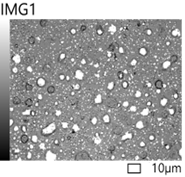
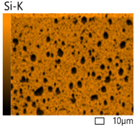
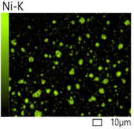
SEM inspection confirms that Ni atoms participate in the formation of clusters/precipitates (Fig. 1). The typical lateral size of the observed features is ~ 1–10 µm, depending on the diffusion temperature and the cooling rate after diffusion annealing. The microstructural observations were performed using a JSM-IT200 SEM. These clusters are interpreted as sinks (getter sites) for oxygen-related species that otherwise contribute to TD generation during subsequent annealings.
Figure 2 presents the EDS analysis of the Ni-related cluster formed in the Si(Ni) sample. In addition to Si and Ni, the cluster contains measurable amounts of technological impurities, primarily oxygen and carbon. In the analysed central region, the atomic percentages are approximately: Si 72.5%, Ni 25.5%, O 1.6%, and C 0.4%. The presence of oxygen (and carbon) inside the Ni-rich cluster supports the interpretation that Ni-related clusters/precipitates incorporate and retain oxygen, thereby decreasing the free oxygen available for thermal-donor generation.
(a)
(b)
(c)
Fig. 1. SEM images of Ni-related clusters/precipitates in Si(Ni) after post-annealing at T = 1000 °C (sample: (a) Cz-Si, (b) KDB-1; (c) Ni diffused in vacuum-sealed quartz ampoules). Scale bars are shown in the micrographs.
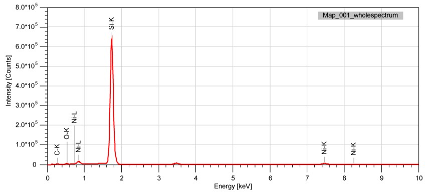
Fig. 2. EDS spectrum acquired from the central region of the Ni-related cluster/precipitate in Si(Ni), showing the elemental composition of the cluster volume.
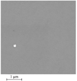
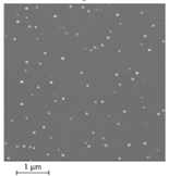
Additional heat treatments lead to observable differences in the current–voltage (I – V) characteristics of the Ni/Si structures. Higher post-annealing temperatures produce a steeper increase in the Schottky-barrier current. Concomitantly, morphological evolution of the Ni layer and near-surface cluster-related features is observed (Fig. 3), indicating thermally activated redistribution/segregation processes. These observations are consistent with the formation and evolution of Ni-related cluster/precipitate regions during post-annealing.
(a)
(b)
Fig. 3. Morphology of the Ni layer on the sample surface: (a) as a deposited Ni layer before post-annealing; (b) after 1 h post-annealing at T = 1000 °C.
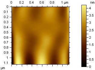
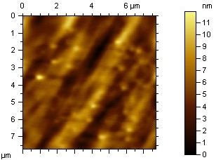
Figure 4 shows clusters formed by Ni atoms in a silicon sample obtained using an atomic force microscope (AFM). When we studied the Ni clusters on the sample surface using a probe, we found that the Schottky barrier properties remained unchanged across all samples.
(a)
(b)
Fig. 4. Atomic force microscopy (AFM) image of the surface topology of samples with clusters of Ni atoms: (a) the surface of the control sample; (b) after temperature treatment T = 1000 °С.
An X-Ray diffractometer device was used to study the electrophysical parameters of nanocluster silicon samples. To determine the nickel-atom clusters in silicon samples treated at different temperatures, the samples were first ground into a powder. Based on the analysis of the experimental results, it was found that nickel atoms form a nanostructured arrangement within the silicon lattice after the high-temperature diffusion process. This, in turn, opens the possibility of creating new types of semiconductor diodes, temperature sensors, and photocells with high sensitivity by introducing nickel atoms into silicon.
Practical note on manufacturability. The present study focuses on the suppression mechanism and the processing window where Ni diffusion forms cluster/precipitate sinks that capture oxygen. If the technology is used as a pregettering step for production wafers (i.e., Ni is not allowed to remain in the final substrate), the Ni-enriched surface region can be removed as a sacrificial layer (grinding and etching as described in section 2) and complemented by standard cleaning/gettering steps used in the semiconductor industry.
As is known from the literature, oxygen atoms in silicon are a source of TDs and also form recombination centres [20–25]. This behaviour is clearly manifested in control samples of silicon (without nickel impurities) [26–29]. Thus, it can be assumed that electrically neutral nickel atoms form clusters that capture and retain a significant concentration of oxygen atoms and other impurities, thereby suppressing the generation of TDs. This ensures the stability of electrical parameters and recombination properties during various heat-treatment processes [30–32].
4. Conclusions
Based on the analysis of the research results, the following conclusions can be drawn:
Impurity nickel atoms in the silicon lattice are mainly electrically neutral, readily forming clusters and deposits.
Clusters of impurity nickel atoms can act as active getter centres for oxygen atoms (and other impurities), thereby significantly suppressing the formation of TDs and recombination centres in the silicon.
The obtained experimental results show that the presence of nickel clusters in silicon leads to stabilisation of the sample electrical parameters regardless of the type of conductivity and resistivity of the material.
Optimal thermodynamic conditions have been determined for obtaining silicon samples with nickel-atom clusters and electrical parameters that remain stable during heat treatment.
At the same time, in nickel-doped samples, electrical parameters practically do not change. The experimental results obtained allow determining the optimal conditions for silicon doping with nickel, which almost completely suppress the generation of TDs.
Electrical parameters of samples doped with impurity nickel atoms and control samples annealed at an annealing temperature T = 1070 °C do not differ significantly. This may be because the concentration of TDs at a given temperature and annealing time will be noticeably lower than the hole concentration in the initial samples. Under the same conditions, the control silicon samples change their conductivity type, becoming n-type with a resistivity of ~ 1.5 ×10³.
Based on the analysis of the research results, the influence of impurity nickel atoms on the generation of TDs has been established, and this influence does not depend on the conditions of nickel diffusion (in air or in evacuated quartz ampoules).
Authors’ statement
Conceptualisation of this study, original writing – initial draft, analysis of results, writing – review & editing, supervision, N.F.Z.; study of TDs in silicon and analysis of the experimental results obtained, K.A.I.; formal X-ray diffraction analysis, Z.T.K.; optical formal analysis, B.K.I.; scanning electron microscope measurements, A.K.; atomic force microscope measurements, A.K.S.; research with literature data on the results obtained, K.Z.; critical revision of the article, discussion and corrections, J.W.
Acknowledgement
The authors express their gratitude to senior lecturer S.V. Koveshnikov for assistance in conducting experiments and discussing the results.
References
[1] Lindroos, J. et al. Nickel: A very fast diffuser in silicon. J. Appl. Phys. 113, 204906 (2013). https://doi.org/10.1063/1.4807799
[2] Shuman, V. B. et al. Solubility of magnesium in silicon. Semiconductors 56, 642–645 (2022). https://doi.org/10.21883/SC.2022.09.54128.9883
[3] Ismaylov, B. K., Zikrillayev, N. F., Ismailov, K. A. & Kenzhaev, Z. T. Clusters of impurity nickel atoms and their migration in the crystal lattice of silicon. Phys. Sci. Technol. 10, 13–18 (2023). https://doi.org/10.26577/phst.2023.v10.i1.02
[4] Esbergenov, D. M., Naurzalieva, E. M. & Tursinbaev, S. A. Enhancing the perfection of a silicon crystal doped with nickel and zinc impurities. East Eur. J. Phys. 4, 172 (2023), https://doi.org/10.26565/2312-4334-2023-4-19
[5] Ismaylov, B., Ismaylov, K., Kamalov, K. & Seytimbetova, G. Suppression of harmful impurity atoms with clusters of nickel impurity atoms in a silicon lattice. AIP Conf. Proc. 2552, 060015 (2022). https://doi.org/10.1063/5.0129486
[6] Yarykin, N. & Weber, J. Electrical activation of interstitial Ni in Cu-doped Si. Phys. Status Solidi A 23, 218 (2021). https://doi.org/10.1002/pssa.202100135
[7] Mil’vidskii, M. G. & Chaldyshev, V. V. Nanometer-size atomic clusters in semiconductors – a new approach to tailoring material properties. Semiconductors 32, 513–522 (1998). https://doi.org/10.1134/1.1187418
[8] Hirose, R, et al. Proximity gettering design of silicon wafers using silicon hydride and hydrocarbon mixture molecular ion implantation technique. Mat. Sci. Semicond. Process. 15, 106063 (2021). https://doi.org/10.1016/j.mssp.2021.106063
[9] Hampel, J., Ehrenreich, P., Wiehl, N., Kratz, J. V. & Reber, S. HCl gas gettering of low-cost silicon. Phys. Status Solidi A 28, 767–770 (2013). https://doi.org/10.1002/pssa.201200885
[10] Vanhellemont, J. SiOx precipitate composition in Si, revisited: Discussion closed? Phys. Status Solidi – Rapid Res. Lett. 10, 597– 602 (2015). https://doi.org/10.1002/pssr.201510313
[11] Bokhan, Yu. I., Kamenkov, V. S. & Tolochko N. K. Dominant factors of laser gettering of silicon wafers. Semiconductors 49, 278–282 (2015). https://doi:10.1134/S1063782615020050
[12] Bakhadyrkhanov, M. K. et al. Silicon photovoltaic cells with clusters of nickel atoms. Appl. Sol. Energy 52, 278–281 (2016). https://doi.org/10.3103/S0003701X1604006X
[14] Supawan, J. et al. Phosphorus gettering of impurities at lowtemperature annealing for enhancing the performance of p-type PERC. AIP Conf. Proc. 2147, 050005 (2019). https://doi.org/10.1063/1.5123854
[15] Kharchenko, V. A. Getters in silicon. Mod. Electron. Mater. 5, 1– 11 (2019). https://doi.org/10.3897/j.moem.5.1.38575
[16] Benkrima, Y. Theoretical study of the electronic properties of nickel clusters. J. Nano- Electron. Phys. 12, 06013 (2020). https://doi.org/10.21272/jnep.12(6).06013
[17] Gui-Yang, H., Yanyao, Z., Yongchun, Li. & Xunxiang, Hu. Firstprinciples investigations of the energetics of He-defect cluster in FCC nickel. J. Appl. Phys. 136, 115107 (2024). https://doi.org/10.1063/5.0220349
[18] Zheng, X. Y., Xie, J., Kong, X. J., Long, L. S. & Zheng, L. S. Recent advances in the assembly of high-nuclearity lanthanide clusters. Coord. Chem. Rev. 378, 222–236 (2019). https://doi.org/10.1016/j.ccr.2017.10.023
[19] Hu, K-Q. et al. Nickel ion induced multistage assembly of Th13 cluster. Nat. Commun. 16, 4000 (2025). https://doi.org/10.1038/s41467-025-58590-z
[20] Vanhellemont, J., De Gryse, O. & Clauws, P. A criterion for the formation of stacking faults at incoherent spheroidal precipitates and application to silicon oxide in silicon. Phys. Status Solidi A 10, 2341–2346 (2006). https://doi.org/10.1002/pssa.200622048
[21] Kissinger, G. et al. Analytical modeling of the interaction of vacancies and oxygen for oxide precipitation in RTA treated silicon wafers. J. Electrochem. Soc. 6, H454–H459 (2007). https://doi.org/10.1149/1.2717492
[22] Newman, R. C. Thermal donors in silicon: Oxygen clusters or selfinterstitial aggregates. J. Phys. C: Solid State Phys. 18, L967 (1985). https://doi.org/10.1088/0022-3719/18/30/001
[23] Markevich, V. P. et al. Electron emission and capture by oxygenrelated bistable thermal double donors in silicon studied with junction capacitance techniques. J. Appl. Phys. 124, 225703 (2018). https://doi.org/10.1063/1.5053805
[24] ur Rehman, A. & Lee, S. L. Advancements in n-Type base crystalline silicon solar cells and their emergence in the photovoltaic industry. Sci. World J. 2013, 470347 (2013). https://doi.org/10.1155/2013/470347
[25] Schön, J. et al. Experimental and theoretical study of oxygen precipitation and the resulting limitation of silicon solar cell wafers. J. Photovolt. 11, 289–297 (2021). https://doi.org/10.1109/JPHOTOV.2020.3044353
[26] Vyvenko, O. F. et al. X-ray beam induced current a synchrotron radiation based technique for the in situ analysis of recombination properties and chemical nature of metal clusters in silicon. Appl. Phys. Lett. 91, 3614 (2002). https://doi.org/10.1063/1.1450026
[27] Astrov, Yu. A. et al. Silicon with an increased content of monoatomic sulfur centers: Sample fabricaton and optical spectroscopy. Semiconductors 47, 211–215 (2013). https://doi.org/10.1134/S1063782613020048
[28] Nasriddinov, S. S. & Esbergenov, D. M. A study of complex defect formation in silicon doped with nickel. Russ. Phys. J. 65, 1559– 1563 (2023). https://doi.org/10.1007/s11182-023-02801-x
[29] Hallam, B. J. et al. Development of advanced hydrogenation processes for silicon solar cells via an improved understanding of the behaviour of hydrogen in silicon. Prog. Photovolt. 28, 1217– 1238 (2020). https://doi.org/10.1002/pip.3240
[30] Kenzhaev, Z. T. et al. Physical mechanisms of gettering properties of nickel clusters in silicon solar cells. Phys. Sci. Technol. 11, 13– 22 (2024). https://doi.org/10.26577/phst2024v11i1a2
[31] Murphy, J. D., Bothe, K., Olmo, M., Voronkov, V. V. & Falster, R. J. The effect of oxide precipitates on minority carrier lifetime in p-type silicon. J. Appl. Phys. 110, 053713 (2011). https://doi.org/10.1063/1.3632067
[32] Bakhadyrkhanov, M. K., Ismailov, K. A. & Kosbergenov, E. Zh. Thermal stability of electrical parameters of silicon crystal doped with nickel during growth. Semicond. Phys. Quantum Electron. Optoelectron. 25, 006–009 (2022). https://doi.org/10.15407/spqeo25.01.006
[13] Kenzhaev, Z. T. et al. Enhancing the efficiency of silicon solar cells through nickel doping. Surf. Eng. Appl. Electrochem. 59, 858–866 (2023). https://doi.org/10.3103/S1068375523060108