In a target location system, the spot size and spot position of the laser light, which are received by a four-quadrant detector, are closely related to the accuracy of the target location. To acquire a pA-level current, according to the characteristics of the signals generated by the four-quadrant detector and the related signal processing circuits, this paper designs signal processing circuits with amplification multiples of 140 dB and 160 dB. Meanwhile, a T‑shaped compensation network is added to the circuit to solve the problem of bandwidth and gain not being increased simultaneously. Theoretical calculations and numerical simulations are carried out to verify this circuit gain, phase margin, and other parameters. Simulation results show that the bandwidth of the signal processing circuit with an amplification of 140 dB is 199.256 kHz, the bandwidth of the signal processing circuit with an amplification of 160 dB is 100 kHz, and the test bandwidth is 96 kHz in 140 dB, which provides a strong support for the calculation of the spot position of the four-quadrant detector.
Introduction
Target positioning is commonly used in underwater laser fuses [1], free-space optical communications [2], atmos-pheric turbulence [3], and laser communication technology [4]. Position-sensitive detectors (PSD), charge-coupled device (CCD) detectors, and quadrant detectors (QD) are frequently used for spot position detection. Compared with PSD and CCD, QD has the advantages of fast response speed, high resolution, high-precision position measurement and wide dynamic range [5–7], which is often used in spot position detection and affects the detection accuracy of spot position.
The system block diagram of target positioning is shown in Fig. 1. First, upon reflection of the laser light from the target object onto the four-quadrant detector, each quadrant generates a distinct current intensity based on the varying intensities of the incident light. These currents then pass through the preamplification circuit, converting the photocurrents generated by the four-quadrant detector into voltages. Then, these voltages subsequently go through the secondary amplification circuit to enhance the initial output voltage. Finally, the amplified signal is collected by a data acquisition card and transmitted via the communication interface between the card and the host computer as a spot detection operation.
Given that the reflected light intensity from the target object is relatively low after laser irradiation and the light intensity illuminating the four-quadrant detector is also low because of environmental influence, as a result of which the current generated by the four-quadrant detector is small.
Therefore, amplifying the current generated by the four-quadrant detector is essential. This amplification aims to fulfil the requirement for acquiring the lowest possible current, thereby enabling high-precision detection of the spot position even under conditions characterised by weak signals.
In target positioning, it is necessary not only to design suitable circuits that can capture the generated current in an accurate and high-speed way, which can improve the capture accuracy of the four-quadrant detector in hardware, but also improve the algorithms to achieve the estimated accuracy of the spot detection. Reference [8] proposed a ground-to-air free-space optical link for a hovering multi-rotor UAV, where a four-quadrant photodetector array is used on the optical receiver to probe the spot. Reference [9] proposed high-precision beam tracking by controlling stepper motors with pulse-width modulated signals. Reference [10] proposed a second-order extended error compensation algorithm based on the Gaussian spot model and incorporated the errors caused by the light source system and environmental changes into the algorithm. Reference [11] proposed a Kalman filtering method to improve the detection accuracy of light spots. Reference [12] proposed a machine learning idea based on [10]. Moreover, the design of the front-end optics in target localization [13], which determines the spot uniformity and the image quality, is also very important.
In this paper, the authors design and analyse a signal processing circuit based on a four-quadrant detector, which enables the conversion of pA-level current to mV-level voltage. Meanwhile, since the signal gain-bandwidth product is a constant value, the bandwidth will decrease when the gain is too large. To solve this problem, a T-shaped compensation network was added to the circuit to compensate for the bandwidth.
The paper is divided into six sections. Section 1 is the introduction, section 2 introduces the measuring principle of the four-quadrant detector, section 3 designs the signal amplification circuit of the four-quadrant detector, section 4 analyses the experimental results of the simulation and section 5 tests the bandwidth and noise of the circuit. Section 6 presents the conclusions.
Measuring principle of the four-quadrant detector
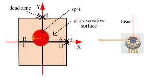
A four-quadrant detector has four photosensitive surfaces with each quadrant separated by a dead zone of equal length [14]. Therefore, a four-quadrant detector can be regarded as a detector composed of four independent photodetectors based on photoelectric effects. Moreover, the photoelectric properties, dark current, and optical characteristics of the photosensitive surface in each quadrant are the same. The accuracy of a four-quadrant detector performance is influenced by several critical factors, including the radius of the detection area, spot radius, noise, width of the dead zone, and laser energy distribution [15–17]. Thus, enhancing the spot detection accuracy for four-quadrant detectors remains a significant area of interest in current research endeavours. The following will discuss the position calculation on the four-quadrant detector of the Gaussian spot model [18–20]. Fig. 2 shows a schematic diagram of the detector spot display.
where h0 is the constant, x0, y0 are the centre of the mass coordinate of the spot, and ω is the radius of the spot. The authors assume that the calculated value of the centre of the light spot on the x-axis and y-axis are σx and σy, respectively, which can be calculated using (2):
The laser beam energy exhibits a Gaussian distribution in practical applications leading to a Gaussian mode spot pattern. However, when lasers are used for a long-distance transmission, they will be scattered because of atmospheric scattering and atmospheric particle scattering, which can alter their original distribution and pattern at the target position. To simplify calculations, the light spot can be regarded as a uniform light spot on the four-quadrant detector within the smaller scale. In that case, when the spot centre illuminates the detector exact centre, each of the four quadrants will generate an equal photocurrent intensity due to the quadrants having the same characteristics [21].
However, as the spot centre moves away from the detector centre, the photocurrent intensity generated in the four quadrants will no longer be equivalent. The photocurrent intensity is closely related to the area covered by the spot in each quadrant [22]. Specifically, the larger the area of the spot in a given quadrant, the stronger the photocurrent generated in that quadrant, whereas a quadrant covering a smaller area generates a weaker photocurrent, so (2) can be calculated according to:
where SA, SB, SC, and SD are the spot area in each quadrant of the four-quadrant detector.
A four-quadrant detector of the Hamamatsu S4349 PIN type is selected for this target experiment. This detector has the advantages of a wide spectral range (190 nm to 1000 nm), high response speed (20 MHz), and a small dead zone width (100 μm). Under the condition of a reverse bias voltage of 5 V, the peak wavelength is 720 nm, the dark current is 0.01 nA, and the responsivity is 0.45 A/W, which has good spectral response characteristics.
Design of the signal processing circuit
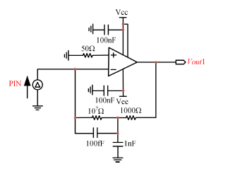
Due to the exceptionally minute photocurrent generated upon laser reflection and detected by the four-quadrant detector, the photocurrent amplification is essential for subsequent data acquisition to be performed at a higher rate. The amplifier circuit consists of two distinct sections, the pre-amplifier circuit and the secondary amplifier circuit. The pre-amplifier circuit, also called the trans-impedance amplifier circuit, primarily converts a weak photocurrent into a corresponding voltage signal. A trans-impedance amplifier circuit adeptly converts current into voltage using an operational amplifier with high input impedance and low output impedance. The gain of this circuit is determined by the feedback resistance, as shown in (6):
where Vout1 is the output voltage of the pre-amplifier, Iin is the photocurrent generated by the detector, and Rf is the value of the feedback resistor.
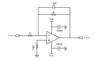
After the initial amplification by the pre-amplifier circuit, the voltage signal output might still not meet the requirements of the data acquisition card. To address this, a secondary amplifier circuit is used for further amplification, allowing for adaptability to varying signal strengths by adjusting the feedback resistor value, thereby achieving higher gain. The formula for calculating gain is shown in (7):
where Vout2 is the output voltage of the secondary amplifier and R1 and R2 are the adjustable resistor values.
For the detector to effectively respond to the laser spot illuminated on the photosensitive surface, the amplification requirement is met and the bandwidth of the laser signal must be less than or equal to the bandwidth of the amplifier closed-loop gain [23].
Design of the pre-amplifier circuit
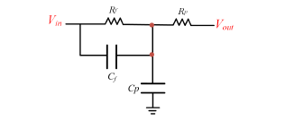
The operational amplifier used in the pre-amplifier circuit is ADI ada4817-2 which has a −3 dB bandwidth of 1050 MHz, a low input bias current of 2 pA, low voltage noise of 4 nF/√Hz and a low current noise of 2.5 fA/√Hz. The purpose of this circuit is to convert the photocurrent to voltage. The amplification is designed to be 140 dB and the value of the feedback resistor is 107 Ω according to the virtual short and open circuits of the operational amplifier. Actually, because of the limitation of the product of gain and bandwidth in operational amplifiers, the gain is increased while the bandwidth decreases. It becomes challenging for the device to achieve both high gain and high bandwidth simultaneously. To solve this problem, a T-type compensation network is added to the feedback loop to compensate for the bandwidth [24]. Fig. 3 shows the schematic diagram of the T-type compensation network, which increases the bandwidth while increasing the gain. When using the network, the circuit needs to be satisfied RfCf = RpCp. Fig. 4 shows the circuit diagram of the pre-amplifier circuit. Two capacitors, each with a value of 100 nF, are positioned in alignment with the input power supply. This strategic placement served to filter the input power supply, thereby enhancing the operational stability of the ADA4817-2 amplifier. An extra phase delay is introduced upon incorporating the feedback resistor into the amplifier circuit. A capacitor (C) is placed parallel to the feedback resistor to mitigate phase delay. The value of this capacitor can be described as C = 1/ωR which is determined by both the signal frequency (ω) and the value (R) of the resistance of the feedback resistor.
Fig. 4. Circuit diagram of the pre-amplifier circuit.
The design of the secondary amplifier circuit
To enhance the multiplexing capability of the amplifier circuit, the secondary amplification circuit is shown in Fig. 5. According to (7), R1 = 100 Ω and R2 = 100 Ω at 1 time and R1 = 100 Ω and R2 = 1000 Ω at 10 times can be easily set. In the secondary amplifier circuit, lmc6482 is used for further amplification, which has a low input current of 20 fA. Two capacitors with a value of 100 nF are also used for the input power supply.
Fig. 5. Circuit diagram of the secondary amplification circuit.
Simulation analysis
The simulation analysis of the pre-amplifier circuit
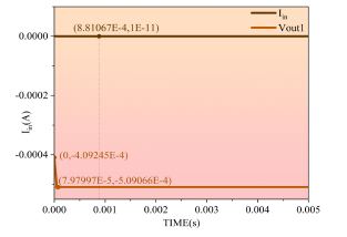
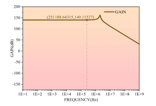
To ascertain the stability of the pre-amplifier circuit, it is assumed that the input signal is a step current signal characterised by an amplitude of 10 pA. When the circuit amplification is 140 dB, the theoretical value of the output voltage should be 100 μA. The instantaneous input and output waveforms are shown in Fig. 6. Under the influence of step current signals, the output waveform exhibits minimal oscillations and the pre‑amplifier circuit is stable in operation. Besides, the peak-to-peak voltage of the simulation output is Vpp = (−409.245 μV) − (−509.066 μV) = 99.82 μV and the gain of the pre-amplifier circuit is A = 20log(Vout1/Iin) = 140 dB, which are very close to the theoretical value. The AC characteristic curve for the pre‑amplifier circuit with a bandwidth of 251.188 kHz and a gain of 140 dB is shown in Fig. 7.
The simulation analysis of the secondary amplifier circuit
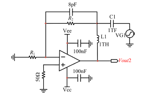
Verification of the stability in the amplifier circuit is essential, differing from the pre-amplifier circuit where stability is confirmed through a step current signal. For the secondary amplifier circuit, ensuring stability involves disconnecting the output from the feedback loop and connecting it with a larger inductor with a value of 1 TH. This configuration also assumes that a step excitation is introduced into the feedback loop via a capacitor valued at 1 TF. The circuit diagram for the stability analysis of the secondary amplifier circuit is shown in Fig. 8. When the input is a DC signal, C1 is equivalent to disconnection, L1 is equivalent to closure, the DC signal is output from the circuit, and the correct DC bias can be obtained. When the input is an AC signal, C1 is equivalent to closure, L1 to disconnection, an AC signal is output from the circuit, and the open-loop gain curve can be obtained. Based on the magnitude of the phase where the frequency is 0 dB on the gain curve, which is crucial for determining the phase margin, this point can be used to indicate how far the system phase response is from the threshold that would cause oscillation. If the phase margin falls within the range from 45° to 90°, it signifies that the circuit is stable. Conversely, if this margin does not lie within this specified interval, the circuit is at risk of experiencing oscillations.
According to the phase margin curve of the amplification circuits with 1 time [Fig. 9(a)] and 10 times [Fig. 9(b)], it is known that the phase margin of the circuit with a 1-time amplification is 60.8° and the phase margin of the circuit with a 10- time amplification is 79.44°, which are both between 45° and 90° so the two amplification circuits are in a stable state. If the amplifier circuit is unstable, one effective approach is introducing a capacitor (Cf) in parallel with the feedback resistor or adding an isolation resistor (Riso). Then, the stability of the circuit can be increased by adding zero compensation [25, 26]. The calculations of Cf and Riso are shown in (8):
Fig. 9. Phase margin curve. (a) Phase margin curve of the secondary amplification circuit with 1 time; (b) phase margin curve of the secondary amplification circuit with 10 times.
Two-stage circuit cascade simulation test
The two-stage amplification circuit diagram for amplifi-cation is shown in Fig. 10. Assuming that the input signal is a step current signal with an amplitude of 10 pA after the signal passes through the two-stage amplification circuit, an instantaneous response waveform of 140 dB [Fig. 11(a)] and 160 dB [Fig. 11(b)] can be obtained respectively. It can be observed that the input current to the PIN is 10−11 A. Amplified by a multiplier of 140 dB, the peak-to-peak value of the output voltage of Vout1 is 100 μV and the peak-to-peak value of the output voltage of Vout2 is 100 μV. Amplified by a multiplier of 160 dB, the peak-to-peak value of the output voltage of Vout1 is 100 μV and the peak‑to-peak value of the output voltage of Vout2 is 1 mV. The actual four-quadrant detector generates much larger currents than 10 pA, possibly up to the μA-level, so that this two-stage amplifier circuit can convert pA to mV.
Fig. 11. Transient response waveforms. (a) Transient response
waveform of an amplification circuit at 140 dB;
(b) transient response waveform of an amplification
circuit at 160 dB.
The gain curves of this two-stage amplifier circuit are shown in Fig. 12(a) and Fig. 12(b). It can be found that at an amplification of 140 dB, the bandwidth can achieve 199.256 kHz. When an amplification is 160 dB, the bandwidth can reach 100 kHz.
Fig. 12. Gain curves. (a) Gain curve for a circuit at 140 dB;
(b) gain curve for a circuit at 160 dB times.
Test of amplifier circuits
The design of PCB
The PCB diagram of the amplifier circuit is shown in Fig. 13. When drawing the diagram, it should be noted that intersections between the positive and negative power lines should be avoided. The cathode of the four-quadrant detector is grounded.
The experimental setup for bandwidth testing includes a power supply (Agilgent N6705B), signal generator (Agilgent 33522A), and oscilloscope. According to the test bandwidth of the RC test circuit [27], a resistor is connected in parallel with a capacitor instead of a four-quadrant at the input of the circuit. Then, the input of the circuit is connected to a signal generator and the output voltage and output frequency of the signal generator are changed. The bandwidth can be calculated by measuring the rise time at different output voltages and output frequencies. The bandwidth (BW) can be estimated by measuring the rise time (τ10~90) of the square wave signal and the formula is calculated as in (9).
\(
\mathrm{BW}=0.349 / \tau_{10-90}
\) (9)
Fig. 14 shows the amplifier circuit board. The detector is mounted on the back of the board. In the actual test, the authors only measured the bandwidth of the amplifier circuit with a 140 dB amplification because the circuit with a 140 dB amplification was already able to detect light with a small amplitude (0.01 Vpp).
The rise time results measured with an amplifier circuit oscilloscope at an input frequency of 3000 Hz and input voltages of 0.08 Vpp, 1 Vpp, 3 Vpp, and 5 Vpp are shown in Fig. 15.
Fig. 15. Rise time results for an input frequency of 3000 Hz and input voltages of 0.08 Vpp, 1 Vpp, 3 Vpp, and 5 Vpp, respectively: (a) the
input frequency is 3000 Hz and the input voltage is 0.08 Vpp; (b) the input frequency is 3000 Hz and the input voltage is 1 Vpp;
(c) the input frequency is 3000 Hz and the input voltage is 3 Vpp; (d) the input frequency is 3000 Hz and the input voltage is 5 Vpp.
The respective bandwidths are estimated to be 98 kHz, 96 kHz, 96 kHz, and 96 kHz. These results demonstrate that the amplifier circuit has a bandwidth of 96 kHz. Since the bandwidth of the circuit is simulated by ignoring the four-quadrant detector and not considering the effect of the bandwidth of the four-quadrant detector itself on the signal chain of the whole amplifier circuit, the bandwidth in the actual test will be smaller than the simulation result.
Noise
Noise testing was performed using the Axopatch data acquisition system. A four-quadrant detector is mounted in the circuit and the noise at different light intensities is measured by varying the light intensity that shines on the four-quadrant detector. The authors measured several sets of noise data at different light intensities and processed them to calculate the root mean square error values (RMSE), and the results are shown in Fig. 16. Based on the test results, it can be seen that the total noise at the output of the four-quadrant detector and the circuit gradually increase as the light intensity increases. The higher error values in the high-intensity region indicate that the noise level fluctuates more in this region and the relationship between noise and light intensity is close to linear. In the low-intensity region, the noise fluctuates less and the relationship between noise and light intensity is close to linear. However, in the middle-intensity section, insufficient data points are collected to rule out anomalies resulting in a tendency for the noise to decrease. At the same time, because of the high input impedance of the circuit, the chip heats up, thus making the thermal noise and the scattering noise of the four-quadrant detector increase significantly when the light intensity increases.
In a targeting system, a four-quadrant detector determines the position based on the magnitude of the incident light intensity. The paper analyses the measuring principle of a four-quadrant detector and designs a signal processing circuit which can get the gain of 140 dB and 160 dB based on the Hamamatsu Si PIN-type four-quadrant detector. After the simulation and analysis, it can be seen that the circuits can get an mV-level output step signal to achieve pA to mV conversion. The circuit bandwidths of 199.256 kHz and 100 kHz can be obtained with amplifications of 140 dB and 160 dB, respectively, by simulation. Moreover, by analysing the phase margins with TINA-Ti, the authors know that phase margins at an amplification of 140 dB and 160 dB are 60.8o and 79.44, respectively. It is known that the circuits designed are capable of stable operation and can also be used for other suitable applications. Finally, the authors built a bandwidth test system to achieve a test bandwidth of the amplified circuit at 140 dB. The result is 96 kHz.
Authors’ statement
Research concept and design, W.S. and X.G.; collection and assembly of data, X.J.; data analysis and interpretation, W.S. and S.X.; writing the article, W.S.; critical revision of the article, S.X. and S.L.; final approval of article, S.X. and S.L.
Acknowledgements
This work was supported by the Chongqing Natural Science Foundation Innovation and Development Joint Fund Project (CSTB2023NSCQ-LZX0173) and the Chongqing Municipal Key Special Project for Technological Innovation and Application Development (CSTB2024TIAD-KPX0109).
References
Xu, G., Zha, B., Yuan, H., Zheng, Z. & Zhang, H. Underwater four- quadrant dual-beam circumferential scanning laser fuze using nonlinear adaptive backscatter filter based on pauseable SAF-LMS algorithm. Def. Technol. 37, 1–13 (2024). https://doi.org/10.1016/j.dt.2023.06.011
Li, Q., Xu, S., Yu, J., Yan, L. & Huang, Y. An improved method for the position detection of a quadrant detector for free space optical communication. Sensors 19, 75 (2019). https://doi.org/10.3390/s19010175
Wang, B., Tan, X., Ma, X. & Li, S. Research on integrated tracking and communication ATP system based on four-quadrant detector. Proc. SPIE 13231, 132312N (2024). https://doi.org/10.1117/12.3040002
Gao, Z.-J, Dong, L.-L. & Xu, W.-H. Design and analysis of displacement measurement system based on the four-quadrant detector. Proc. SPIE 8905, 890531 (2013). https://doi.org/10.1117/12.2040172
Wu, X. et al. Study on the influence of random phase interference on the positioning performance of a four-quadrant detector. IEEE Photon. J. 16, 1–6 (2024). https://doi.org/10.1109/jphot.2024.3408285
Qiu, Z., Jia, W., Ma, X., Zou, B. & Lin, L. Neural-network-based method for improving measurement accuracy of four-quadrant detectors. Appl. Opt. 61, F9–F14 (2022). https://doi.org/10.1364/ao.444731
Safi, H., Dargahi, A. & Cheng, J. Beam tracking for UAV-assisted FSO links with a four-quadrant detector. IEEE Commun. Lett. 25, 3908–3912(2021). https://doi.org/10.1109/lcomm.2021.3113699
Ke, X. & Liang, H. Airborne laser communication system with automated tracking. Int. J. Opt. 2021, 9920368 (2021). https://doi.org/10.1155/2021/9920368
Bao, R. et al. Research on high-precision position detection based on a driven laser spot in an extreme ultraviolet light source. Photonics 11, 75 (2024). https://doi.org/10.3390/photonics11010075
Wang, X. et al. A method for improving the detection accuracy of the spot position of the four-quadrant detector in a free space optical communication system. Sensors 20, 7164 (2020). https://doi.org/10.3390/s20247164
Cao, W., Huang, Y., Fan, K.-C. & Zhang, Y. A novel machine learning algorithm for large measurement range of quadrant photodetector. Optik 227, 165971 (2021). https://doi.org/10.1016/j.ijleo.2020.165971
Gu, S., Guo, Y. & Ju, Y. Design of optical quality detection system for four-quadrant detector lens. Acta Opt. Sin. 42, 0222001 (2022). (in Chinese) https://doi.org/10.3788/aos202242.0222001
Lu, B.-Y. ANFIS‐based controlled spherical rotator with quadrant photodiode to improve position detection accuracy. IET Optoelectron. 18, 146–156 (2024). https://doi.org/10.1049/ote2.12127
Li, D. & Zhang, Y. Research on factors influencing the positioning accuracy of four-quadrant detector. J. Phys.: Conf. Ser. 1983, 012087 (2021). https://doi.org/10.1088/1742-6596/1983/1/012087
Qiu, Z., Lin, L. & Chen, L. An active method to improve the measurement accuracy of four-quadrant detector. Opt. Lasers Eng. 146, 106718 (2021). https://doi.org/10.1016/j.optlaseng.2021.106718
Wang, X., Su, H., Liu, G., Han, J. & Wang, R. Investigation of high- precision algorithm for the spot position detection for four-quadrant detector. Optik 203, 163941 (2020). https://doi.org/10.1016/j.ijleo.2019.163941
Xiao, M., Zhang, Y. & Li, H. High-precision spot positioning algorithm based on fourquadrant detector. J. Phys.: Conf. Ser. 1633, 012122 (2020). https://doi.org/10.1088/1742-6596/1633/1/012122
Zhang, J. et al. Quadrant response model and error analysis of four- quadrant detectors related to the non-uniform spot and blind area. Appl. Opt. 57, 6898–6905 (2018). https://doi.org/10.1364/ao.57.006898
Zhang, J. et al. A calibration and correction method for the measurement system based on four-quadrant detector. Optik 204, 164226 (2020). https://doi.org/10.1016/j.ijleo.2020.164226
Wang, X., Su, X., Liu, G., Han, J. & Wang, R. Research on Photoelectric Signal Preprocessing of A Four-Quadrant Detector in Free Space Optical Communication System. in 2020 IEEE 5th International Conference on Signal and Image Processing (ICSIP) 628–632 (IEEE, 2020). https://doi.org/10.1109/ICSIP49896.2020.9339342
Wu, X.-J., Cui, J.-Y., Xu, C.-X., Zheng, W. & Zheng, Y.-C. The design of laser detection circuit with high reliability and large dynamic range based on APD. Proc. SPIE 10846, 108461U (2018). https://doi.org/10.1117/12.2505189
Mohammadi, M., Karimi, G. & Sarabi, H. G. Design of a microstrip Wilkinson power divider using a low pass filter with the particle swarm optimization algorithm. Sci. Rep. 14, 17637 (2024). https://doi.org/10.1038/s41598-024-66544-6
Shlyonsky, V. & Gall, D. The OpenPicoAmp-100k: an open-source high-performance amplifier for single channel recording in planar lipid bilayers. Pflug. Arch. Eur. J. Physiol. 471, 1467–1480 (2019). https://doi.org/10.1007/s00424-019-02319-7