
Heterostructure of graphene with a two-dimensional crystalline molybdenum trioxide (MoO3) layers
Paweł Krukowski1*
Michał Piskorski1
Maciej Rogala1
Paweł Dąbrowski1
Iaroslav Lutsyk1
Witold Kozłowski1
Patryk Krempiński1
Maxime Le Ster1
Aleksandra Nadolska1
Beata Łuszczyńska2
Paweł J. Kowalczyk1
- Department of Solid State Physics, Faculty of Physics and Applied Informatics, University of Lodz, ul. Pomorska 149/153, 90–236 Łódź, Poland
- Department of Molecular Physics, Lodz University of Technology, ul. Żeromskiego 116, 90–924 Łódź, Poland
Article Info
Received 10 Jun. 2024
Received in revised form 04 Jan. 2025
Accepted 14 Apr. 2025
Available on-line 13 May 2025
Keywords: graphene; molybdenum trioxide; heterostructure; AFM.
Abstract
The heterostructure consisting of graphene and two-dimensional (2D) crystalline molybdenum trioxide (MoO3) layers was fabricated through a wet transfer method using a polymer to transfer the MoO3 layers from the mica crystal surface. Using a heating plate method, this crystalline MoO3 was initially grown on mica under normal atmospheric air conditions. Furthermore, the authors demonstrated that the only MoO3 phase forms on the molybdenum foil following annealing in air, as confirmed by X-ray photoelectron spectroscopy (XPS) study. The resulting graphene heterostructure was examined using optical and atomic force microscopy (AFM). The fabrication method introduced here offers a cost-effective alternative to the more costly and complex ultra-high vacuum techniques used for epitaxial layer fabrication. This graphene heterostructure holds potential as a conductive and transparent anode for the organic light-emitting diode (OLED) technology.
Introduction
Since the breakthrough discovery of graphene, two-dimensional (2D) materials have attracted much attention due to their extraordinary properties compared with their bulk counterparts [1, 2]. The unique properties of 2D materials lead to the development of various emerging applications in electronics, sensors, and optoelectronics [3]. In particular, graphene can be considered as an electrode in the construction of organic light-emitting diode (OLED) [4, 5] due to its high electrical conductivity, transparency in the visible range, and flexibility. However, there is a major problem regarding the possibility of using graphene as an anode in the OLED. Namely, the work function of pristine graphene is too low to be used as an anode [5, 6]. Graphene, depending on the number of layers and the presence of defects, has a work function in the range of 3.9–4.8 eV [7, 8]. To effectively act as an anode in the OLED, the work function of graphene should be higher than 5.2 eV [9]. Deposition of transition metal oxide (TMO) exhibiting a high working function, such as molybdenum oxide and rhenium oxides, is an effective method of work function enhancement. In previous research, the authors showed that graphene and graphite can be greatly enhanced by depositing molybdenum trioxide (MoO3) [10–13] and dirhenium heptoxide (Re2O7) [7, 9, 14] in ultra-high vacuum conditions. However ultra-high vacuum deposition process requires a complicated and expensive scientific apparatus. In contrast, here, the authors show that the process of MoO3 deposition on graphene can be done more easily, at lower cost, and in ambient atmospheric conditions, using a thermal heating plate method and polymer transfer.
MoO3 has been a subject of intense research leading to the fabrication of 2D material systems with great application potential in organic photovoltaics [15], smart windows [16], energy catalysis [17], photocatalytic activity [18], electrodes for rechargeable batteries [19], gas sensors [20], OLEDs [21], and others [22]. Formerly, it was reported that high-quality crystalline MoO3 layers with thicknesses ranging from 1.4 nm (bilayers) up to several nanometres can be synthesized on mica (001) in ambient conditions using a straightforward heating plate method [23, 24]. The method based on epitaxial van der Waals growth allows the formation of large crystalline layers with lateral dimensions of tens of millimeters on mica [23]. In this method, a freshly cleaved mica is put directly on a molybdenum foil heated with a heating plate at a relatively low temperature of 540 °C under ambient atmospheric conditions. The heating process of a molybdenum foil in air causes the formation of molybdenum oxide clusters on this foil. The molybdenum oxide clusters exhibit a much lower sublimation temperature than elemental molybdenum. At a temperature of 540 °C, molybdenum oxide clusters sublimate from molybdenum foil, leading to deposition of molybdenum oxide on mica placed above molybdenum foil. Since mica is an inert and dangling-bond-free substrate that allows high diffusion of molybdenum oxide clusters, the formation of 2D islands with large lateral dimensions is observed. X-ray photoelectron spectroscopy (XPS) and Raman studies showed that α-MoO3 phase is formed on mica using a heating plate method [23]. Recently, it was shown that the direct transformation of crystalline MoO3 on mica by sulfurization at 500 –600 °C into MoS2 nanosheets can be performed simply and effectively [25]. It should be noted that the heating plate method can also be used for the growth of MoO3 on different substrates, including Si [26], Au [27], and SiO2 [28].
In this paper, the authors demonstrate the growth of MoO3 layers on mica using the heating plate method in air and the transfer of crystalline MoO3 layers from mica to graphene using a polydimethylsiloxane (PDMS) stamp. Thus, the heterostructure of graphene with a 2D crystalline MoO3 layer dedicated to OLED device as a transparent anode has been presented.
Experimental methods
To fabricate 2D crystalline MoO3 layers, a clean, freshly exfoliated high-quality muscovite mica (HQ graphene) was used. The deposition of MoO3 on mica was carried out from molybdenum foil with a thickness of about 0.05 mm (MaTecK GmbH), heated by a heating plate to a tem-perature of 450 °C in the air. Hydrogen-intercalated double-layer graphene (here referred to as graphene) grown on a transparent 6H-SiC(0001) substrate (Institute of Electronic Materials Technology, Poland) [29] was used as a substrate for transferring MoO3 from mica. To transfer MoO3 layers from mica to graphene, a highly hydrophobic polymer stamp made of commercially available visco-elastic PDMS (Gelfilm by Gelpak) was used.
To characterise the morphology of MoO3 on mica and MoO3 on graphene atomic force microscopy (AFM), a study was performed under ambient air conditions in a semi-contact mode by the use of an Ntegra Aura microscope with an NSG01/Au cantilever (NT-MDT). Optical microscope images were collected by an upright metallurgical microscope (Huvitz).
The XPS analysis was performed using a non-monochromatic X-ray radiation at 1253.64 eV (Mg Kα) from a DAR 400 source lamp (Omicron). This setup was paired with a Phoibos 150 hemispherical electron energy analyser (SPECS) and a 2D-CCD detector. Background subtraction was carried out using the Shirley method.
Results
The authors first conducted an XPS study to determine the stoichiometry of pristine molybdenum foil and molyb-denum foil after annealing. It was crucial to examine the oxide phase formed on the foil surface after prolonged heating and understand how the annealing treatment changes the properties of the molybdenum foil. Fig. 1 shows the XPS spectra of the Mo 3d core level for both pristine molybdenum foil and foil annealed at 450 °C for 12 h. During peak fitting of the Mo 3d spectra, a charac-teristic 3d5/2–3d3/2 doublet, corresponding to a single oxidation state, was fixed with an energy splitting of 3.1 eV and relative integrated peak areas of 3:2 due to spin-orbit coupling. For the oxide molybdenum component, peak fitting was performed using mixed Gaussian/Lorentzian line shapes [GL(70)] with a full width at half maximum (FWHM) ranging from 1.2 to 1.4 eV. For the metallic molybdenum component, an asymmetric Lorentzian line shape, specifically LA(1.1, 5, 11), was used to fit the peak. This approach accounts for the inherent asymmetry observed in the spectral features characteristics of metallic states. The FWHM parameter was fixed at 1.0 eV.
For pristine foil, the XPS spectra peak fitting indicates the presence of 3d5/2 and 3d3/2 spin-orbit doublet peaks at binding energies of 227.8 and 230.9 eV, respectively. This confirms that the pristine foil contains metallic components. Additionally, peaks at binding energies of 232.4 and 235.5 eV were observed, indicating the presence of the MoO3 phase in the pristine foil. This agrees with reference works from the literature and the authors’ previous reports [10, 13].
The stoichiometry of the surface of molybdenum foil changes radically after heating at 450 °C for 12 h in ambient air. After annealing, the molybdenum foil shows only the presence of 3d5/2 and 3d3/2 spin-orbit doublet peaks at binding energies of 232.4 and 235.5 eV, respectively. This indicates the presence of only the MoO3 phase on the surface of the molybdenum foil after annealing. This observation proves that only MoO3 clusters from annealed molybdenum foil can sublimate, leading to the formation of only MoO3 layers on mica.
Next, the authors slightly modified the procedure of MoO3 growth on mica presented by Molina-Mendoza et al. [23]. First, an annealed molybdenum foil was placed on the heating plate at 450 °C under ambient air conditions. Then, the freshly cleaved exfoliated mica was placed at a distance of about 1 mm from molybdenum foil using ceramic spacers to allow ambient air to circulate for 24 h. After that, mica was removed from the heating plate, cooled down to room temperature, and characterised by an optical micro-scope and AFM.
In the second step of heterostructure fabrication, a highly hydrophobic polymer stamp of PDMS was placed on the surface of MoO3 layers grown on mica and pressed against the MoO3 layers. The MoO3 layers and PDMS polymer were bonded during compression due to adhesion bonds. In the third step, the surface of mica, together with the MoO3 layers and the polymer stamp, was placed in demineralized water. Due to the highly hydrophilic nature of the mica surface, water molecules penetrated the region between the mica and MoO3 layers. This caused rapid, spontaneous detachment of MoO3 layers from the mica surface. As a result, MoO3 layers adsorbed onto a polymer stamp were obtained. The polymer stamp, together with the MoO3 layers, was dried gently in a nitrogen stream. Then, the dried polymer stamp and MoO3 layers were pressed against the graphene. In the final step of heterostructure fabrication, the polymer stamp was gently detached from the graphene surface. Due to the greater adhesion of the MoO3 layers to graphene than to the polymer stamp, most of the MoO3 layers remained on the surface of graphene. As a result of the wet transfer process, the authors obtained a heterostructure of graphene with crystalline MoO3 layers. An optical microscope and an AFM then characterised the graphene heterostructure.
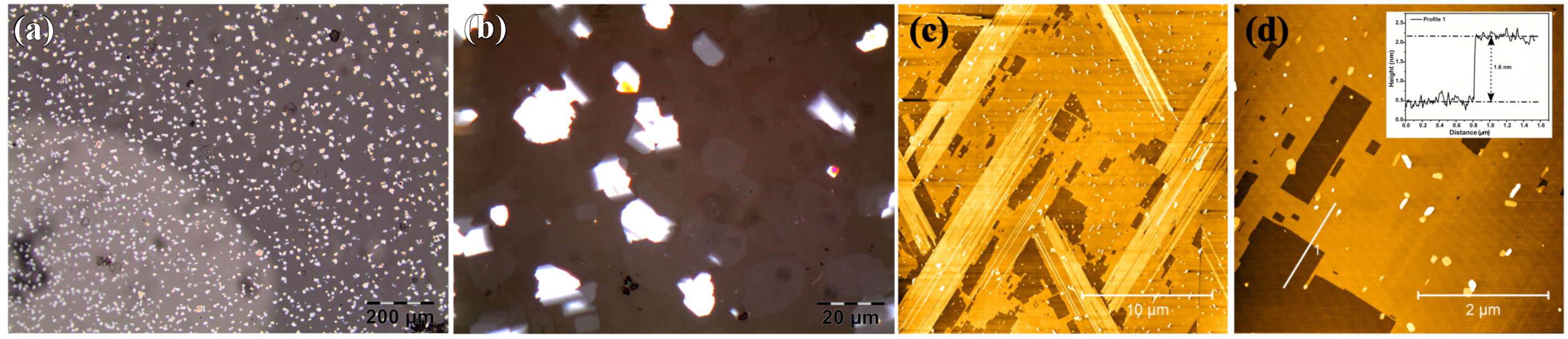
Fig. 2(a) and Fig. 2(b) show optical microscope images of MoO3 macroscopic crystals grown on a mica surface from molybdenum foil using the heating plate method at 450 °C for 24 h under ambient air conditions. The mica substrate symmetry determined the growth of MoO3 crystals. Additionally, Fig. 2(c) shows extended 2D ultra-thin layers of MoO3 on mica. Since mica is transparent, the ultra-thin layers are poorly visible. More details about ultra-thin layers can be obtained from AFM study. Figures 2(c) and (d) show AFM images of MoO3 ultra-thin layers grown on mica. The AFM observation shows the formation of high-quality crystalline layers reflecting mica symmetry, with a thickness ranging from 1.6 nm (bilayer) to several nanometers on the surface of mica. Fig. 2(d) shows an AFM image of a MoO3 bilayer with a thickness of 1.6 nm. The authors define a MoO₃ bilayer as consisting of two octahedral layers stacked via van der Waals inter-actions, with each layer connected to the adjacent one. This bilayer structure extends over two unit layers along the b‑direction resulting in a total thickness of 13.8 Å, corre-sponding to the full b-axis lattice parameter of bulk α‑MoO₃. It was noticed that the MoO3 bilayer formation on mica is preferred in the deposition process at 450 °C for 24 h. Additionally, the authors noticed that longer deposi-tion time leads to thicker MoO3 layers. It should be noted that, for shorter deposition time, the authors occasionally observed the formation of very small, atomically-flat islands with a thickness of about 0.8 nm (monolayer).
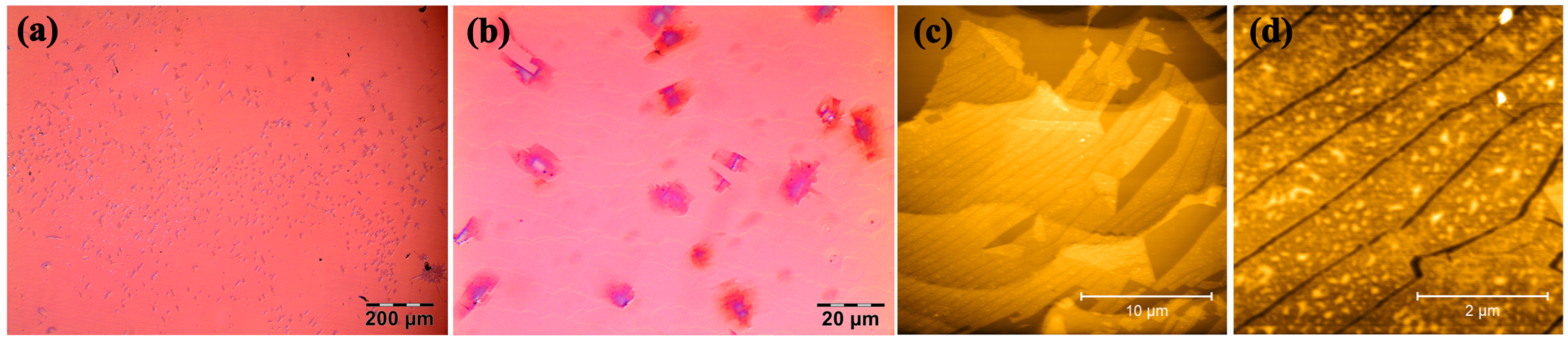
Figures 3(a) and (b) show optical microscope images of heterostructure consisting of MoO3 transferred from mica to graphene surface by a PDMS stamp. It was noticed that both macroscopic crystals and ultra-thin layers of MoO3 were transferred. However, the transfer process reduced the number of macroscopic MoO3 crystals and ultra-thin layers. Additionally, Fig. 3(b) shows extended 2D ultra-thin layers of MoO3 on mica. Since graphene on SiC is transparent, thus ultra-thin layers are very poorly visible in optical images, as well. Figures 3(c) and (d) show AFM images of MoO3 ultra-thin layers transferred from mica to graphene exhibiting different types of defects such as cracks, wrinkles, and bubbles. The images also evidence that the transfer process affected considerably the MoO3 ultra-thin layers. In the transfer process, the ultra-thin layers were torn into smaller pieces. Fig. 3(d) shows a torn layer with a thickness of 3.3 nm (four layers). The existence of bubbles is typical in heterostructure fabricated by the wet transfer method using polymer stamp. This is an effect of trapping either air or hydrocarbon residues between the substrate and the 2D material [30].
Conclusions
XPS study shows the formation of only MoO3 phase on the molybdenum foil surface after annealing of molybdenum foil under ambient air conditions. The authors fabricated a graphene heterostructure with 2D crystalline ultra-thin MoO3 layers by a wet transfer process of MoO3 using a PDMS stamp from a mica crystal surface. The crystalline ultra-thin MoO3 layers were grown on mica under ambient air conditions using a heating plate method. The obtained graphene heterostructure was characterised by the optical microscope and AFM techniques. The presented fabrica-tion method can be a cheap alternative to the expensive and complicated fabrication method of epitaxial layer growth in ultra-high vacuum conditions. Additionally, the authors’ graphene heterostructure can be considered as a conductive and transparent anode in the construction of OLED.
Authors’ statement
Research concept and design, P.K.; collection of data, P.K., M.P., M.R., P.D., I.L., W.K., P.Kre., M.L.S., and A.N.; data analysis and interpretation, P.K., M.P., and M.R.; critical revision of the article, B.Ł. and P.J.K.; final approval of article, B.Ł. and P.J.K.
Acknowledgements
This work was financially supported by the National Science Centre (Poland) under grant 2020/37/B/ST5/03929.
References
-
Zeng, M., Xiao, Y., Liu, J., Yang, K. & Fu, L. Exploring two- dimensional materials toward the next-generation circuits: From monomer design to assembly control. Chem. Rev. 118, 6236–6296 (2018). https://doi.org/10.1021/acs.chemrev.7b00633
-
Shanmugam, V. et al. A review of the synthesis, properties, and applications of 2D materials. Part. Part. Syst. Charact. 39, 2200031 (2022). https://doi.org/https://doi.org/10.1002/ppsc.202200031
-
Glavin, N. R. et al. Emerging applications of elemental 2D materials. Adv. Mat. 32, 1904302 (2020). https://doi.org/https://doi.org/10.1002/adma.201904302
-
Kwon, O. E. et al. A prototype active-matrix OLED using graphene anode for flexible display application. J. Inf. Disp. 21, 49–56 (2020). https://doi.org/10.1080/15980316.2019.1680452
-
Meyer, J. et al. Transition metal oxides for organic electronics: Energetics, device physics and applications. Adv. Mat. 24, 5408– 5427 (2012). https://doi.org/10.1002/adma.201201630
-
Naghdi, S., Sanchez-Arriaga, G. & Rhee, K. Y. Tuning the work function of graphene toward application as anode and cathode. J. Alloys Compd. 805, 1117–1134 (2019). https://doi.org/10.1016/j.jallcom.2019.07.187
-
Krukowski, P. et al. Graphene on quartz modified with rhenium oxide as a semitransparent electrode for organic electronics. Opto- Electron. Rev. 30, e141953 (2022). https://doi.org/10.24425/opelre.2022.141953
-
Yang, N. et al. Design and adjustment of the graphene work function via size, modification, defects, and doping: A first-principle theory study. Nanoscale Res. Lett. 12, 642 (2017). https://doi.org/10.1186/s11671-017-2375-3
-
Krukowski, P. et al. Characterisation of a graphene/NPB structure with Re2O7 as an interfacial layer for OLED application. Opto- Electron. Rev. 32, e147913 (2024). https://doi.org/10.24425/opelre.2024.148441
-
Kowalczyk, D. A. et al. Local electronic structure of stable monolayers of α-MoO3−x grown on graphite substrate. 2D Mater. 8, 25005 (2020). https://doi.org/10.1088/2053-1583/abcf10
-
Kowalczyk, D. A. et al. Two-dimensional crystals as a buffer layer for high work function applications: The case of monolayer MoO3. ACS Appl. Mater. Interfaces 14, 44506–44515 (2022). https://doi.org/10.1021/acsami.2c09946
-
Kowalczyk, P. J. et al. Flexible photovoltaic cells based on two- dimensional materials and their hybrids. Prz. Elektrotech. 98, 117– 120 (2022). [in Polish] https://doi.org/10.15199/48.2022.02.26
-
Nadolska, A. et al. Electrostimulation and nanomanipulation of two- dimensional MoO3-x layers grown on graphite. Crystals (Basel) 13, 905 (2023). https://doi.org/10.3390/cryst13060905
-
Krukowski, P. et al. Work function tunability of graphene with thermally evaporated rhenium heptoxide for transparent electrode applications. Adv. Eng. Mater. 22, 1900955 (2020). https://doi.org/10.1002/adem.201900955
-
Gong, Y. et al. Diverse applications of MoO3 for high performance organic photovoltaics: fundamentals, processes and optimization strategies. J. Mater. Chem. A 8, 978–1009 (2020). https://doi.org/10.1039/C9TA12005J
-
Morita, M. et al. Chromogenic amorphous MoO3–x nanosheets and their nanostructured films for smart window applications. ACS Appl. Nano Mater. 4, 8781–8788 (2021). https://doi.org/10.1021/acsanm.1c01428
-
Avani, A. V & Anila, E. I. Recent advances of MoO3 based materials in energy catalysis: Applications in hydrogen evolution and oxygen evolution reactions. Int. J. Hydrog. Energy 47, 20475–20493 (2022). https://doi.org/https://doi.org/10.1016/j.ijhydene.2022.04.252
-
Al-Alotaibi, A. L. et al. Synthesis and characterization of MoO3 for photocatalytic applications. J. Inorg. Organomet. P. 31, 2017–2029 (2021). https://doi.org/10.1007/s10904-021-01939-w
-
Tang, K., Farooqi, S. A., Wang, X. & Yan, C. Recent progress on molybdenum oxides for rechargeable batteries. ChemSusChem 12, 755–771 (2019). https://doi.org/https://doi.org/10.1002/cssc.201801860
-
Malik, R., Joshi, N. & Tomer, V. K. Advances in the designs and mechanisms of MoO3 nanostructures for gas sensors: A holistic review. Mater. Adv. 2, 4190–4227 (2021). https://doi.org/10.1039/D1MA00374G
-
Li, Y. et al. Ultrathin MoO3 layers in composite metal electrodes: Improved optics allow highly efficient organic light-emitting diodes. Adv. Opt. Mater. 7, 1801262 (2019). https://doi.org/https://doi.org/10.1002/adom.201801262
-
Arash, A. et al. Large-area synthesis of 2D MoO3−x for enhanced optoelectronic applications. 2D Mater. 6, 35031 (2019). https://doi.org/10.1088/2053-1583/ab1114
-
Molina-Mendoza, A. J. et al. Centimeter-scale synthesis of ultrathin layered MoO3 by van der Waals epitaxy. Chem. Mat. 28, 4042–4051 (2016). https://doi.org/10.1021/acs.chemmater.6b01505
-
Wang, D. et al. Van der Waals epitaxy of ultrathin α-MoO3 sheets on mica substrate with single-unit-cell thickness. Appl. Phys. Lett. 108, 053107 (2016). https://doi.org/10.1063/1.4941402
-
Carrascoso, F. et al. Direct transformation of crystalline MoO3 into few-layers MoS2. Materials 13, 2293 (2020). https://doi.org/10.3390/ma13102293
-
Puebla, S. et al. In-plane anisotropic optical and mechanical properties of two-dimensional MoO3. NPJ 2D Mater. Appl. 5, 37 (2021). https://doi.org/10.1038/s41699-021-00220-5
-
Zhang, C. et al. Modified hot plate method for synthesizing MoO3 nanoplates. Chin. J. Chem. Phys. 36, 242–248 (2023). https://doi.org/10.1063/1674-0068/cjcp2111238
-
Puebla, S., Mariscal-Jiménez, A., Galán, R. S., Munuera, C. & Castellanos-Gomez, A. Optical-based thickness measurement of MoO3 nanosheets. Nanomaterials 10, 1272 (2020). https://doi.org/10.3390/nano10071272
-
Strupinski, W. et al. Graphene epitaxy by chemical vapor deposition on SiC. Nano Lett. 11, 1786–1791 (2011). https://doi.org/10.1021/nl200390e
-
Frisenda, R. et al. Recent progress in the assembly of nanodevices and van der Waals heterostructures by deterministic placement of 2D materials. Chem. Soc. Rev. 47, 53–68 (2018). https://doi.org/10.1039/C7CS00556C