Multimode interference (MMI) waveguides are favoured for their wide bandwidth, extensive fabrication tolerance, high stability, effective light confinement, and minimal transmission loss. In this study, the authors propose a numerical design of an optical power splitter based on restricted interference (RI) mechanisms using silicon-on-insulator waveguides, where the precise positioning of input pairs and subsequent adjustment of the MMI region length are essential aspects. The RI-MMI configuration facilitates the reduction of the MMI length due to the applied interference theory. The authors’ design undergoes a rigorous simulation and optimization using a highly accurate three-dimensional beam propagation method (3D-BPM) simulation method to ensure optimal performance. Simulation results confirm the authors high-performance design with low excess loss (< 2.7 dB), small relative phase difference (< 2%), negligible residual (< −18 dB), excellent coupling ratio (−0.09 dB to 0.05 dB), and high balance factor (< −17 dB) across the wide range of 100 nm (1500 nm–1600 nm). Furthermore, the authors’ optimized design exhibits a width tolerance of ± 2.1 μm and a height tolerance of ± 10 nm. Notably, the core component of the splitter is housed within an extremely compact footprint area of 6 μm × 65 μm. These exceptional characteristics position the authors’ proposed device as highly promising for large-scale integrated optical circuits, as well as photonic neural networks in ultrawideband telecom applications.
Introduction
Photonic integrated circuits are becoming increasingly vital in advancing modern optical technologies. As the demand for high-speed and efficient optical communication grows, the development of core components within these circuits is essential. In the realm of photonic integrated circuits, optical power splitters are crucial components for constructing complex optical interconnects and networks, such as optical switches [1], ring lasers [2], optical modulators [3, 4], polarization scramblers [5], and photonic neural networks (PNNs) [6–8]. On various platforms, silicon-on-insulator (SOI)-based optical power splitters/couplers are particularly promising for large-scale photonic integration due to several significant advantages. These benefits include high refractive index contrast, which leads to low bending loss and strong guided confinement, as well as low infrared absorption, enabling low-loss propagation. Additionally, this material platform is compatible with a complementary metal oxide semiconductor (CMOS) technology, allowing for cost-effective mass production [9–11].
There are numerous approaches for designing optical power splitters on the silicon photonics platform. For instance, Y-junction couplers provide a simple geometrical structure but require complicated mask designs and suffer from high scattering at joint junctions [12–14]. Adiabatic and directional couplers offer low-loss performance but demand precise coupling gap designs [15–17]. Recently, two promising methods for creating broadband and highly compact 3-dB power splitters have emerged: using subwavelength grating-assisted silicon waveguides [18–20] and employing inverse design with deep learning techniques [21–23]. However, these approaches either need high-resolution design procedures for nanoscale grating structures or require extensive training time for AI models. Additionally, the compact and intricate designs result in expensive mask patterning and high fabrication costs [24, 25].
In silicon photonic waveguides, multimode interference (MMI) couplers are crucial for creating advanced functional devices, such as optical logic gates [26, 27], thermo-optic switches [28], and particularly arbitrary-ratio optical power splitters [29, 30]. Recently, a 3-dB power splitter using a 1 × 2 MMI coupler designed for dual-band wavelengths, specifically 1.55-μm and 2-μm, has been introduced [31]. However, this splitter is limited as it operates with only one input port.
Due to these significant characteristics, MMI couplers have been employed in the development of advanced photonic integrated circuits and optical communications. However, the proposed MMI couplers typically are based on the general interference regime, resulting in a consider-able overall device length. This paper introduces a numerical simulation design for a 3-dB optical power splitter that utilizes a 2 × 2 MMI coupler specifically engineered with a restricted interference regime to shorten the multimode interference region. The simulation results, derived from the three-dimensional beam propagation method (3D-BPM), demonstrate an MMI-based power splitter with reduced length, low loss, and high balance across a broad wavelength range.
Optimized design and characteristic simulation
Fig. 1 illustrates a principal diagram of a 3-dB optical power splitter based on a 2 × 2 MMI coupler operating under transverse electric (TE) polarization. Fig. 1(a) specifically shows the side view of the proposed 3-dB splitter, and Fig. 1(c) shows the mode profile of the fundamental mode TE0 for the input light at the single-mode access waveguide (Port1). In this design, tapers are used as two input ports and two output ports instead of traditional rectangular access waveguides. This aims to improve the coupling efficiency between the access single-mode waveguides and the multimode region [32].
Fig. 1.The design structure of the 3-dB power splitter based on a 2 × 2 MMI in the restricted interference (RI) mechanism using SOI
waveguide platform: (a) schematic diagram; (b) cross-sectional view, and (c) computed mode profile of the access waveguide.
The entire device is constructed on a SOI material plat-form, featuring a silicon (Si) guiding layer with a thickness of h = 220 nm and a 3 μm-thick buried oxide (BOX) layer of silica (SiO2), derived from a standard SOI wafer using the CMOS semiconductor manufacturing technology. The refractive indices of the silicon core and the cladding oxide layer are considered constants at nr = 3.47 and nc = 1.444, respectively, as determined by the Sellmeier model [33], with negligible variations in the third telecom window [34, 35]. Additionally, the silicon core layer is surrounded by the cladding oxide layer, forming channel waveguides.
In the central section of the device, the 2 × 2 MMI coupler has an initial multimode region width WMMI = 5.4 μm. The tapers are designed in the shape of an isosceles trapezoid, characterized by a narrower bottom base width of 450 nm, a broader top base width of 900 nm, and a length of 15 μm. These dimensions were initially selected. The central axis of the MMI coupler in the propagation direction serves as the axis of symmetry. The narrower bottom bases at both inputs and outputs are coupled to 450 nm-thickness access waveguides to achieve high efficiency in the single-mode waveguide regime, as shown in Fig. 1(a).
To reduce the multimode length required to generate two mirrored fold-images, this paper proposes using a restricted interference regime where the input and output ports are positioned at approximately y = ±WMMI / 6 [36]. According to the RI theory, at these positions, the overlap between the symmetric input field and the antisymmetric mode fields vanishes. This results in a periodic and paired reproduction of single images of the input field at the MMI region as much as multiple of a critical length, L = p(Lπ), with p = {0, 1, 2…} as a non-negative integer, where the critical length Lπ is the half-beat length of the MMI coupler which is defined by the following formula [36]:
where β0, β1 are corresponding to the propagation constants of the fundamental and first-order modes, respectively; λ0= 1550 nm is the operation wavelength in the waveguides, and We is the effective width of the MMI coupler which is calculated by the following formula under the TE polarization state for the channel waveguide [36, 37]:
\(
where β0, β1 are corresponding to the propagation constants of the fundamental and first-order modes, respectively; λ0= 1550 nm is the operation wavelength in the waveguides, and We is the effective width of the MMI coupler which is calculated by the following formula under the TE polarization state for the channel waveguide [36, 37]:
\) (2)
Here, neff represents the effective refractive index of the silicon core layer in the channel-formed multimode waveguide, which can be obtained from the mode solver in the BPM numerical simulation.
Following the restricted interference theory, the single fold-images (direct or inverted images) are reproduced at the length LMMI = p(Lπ), with p as the positive integer. In addition, the paired interference regime also exhibits two differently mirrored images at minimal lengths of the multimode region LMMI = Lπ / 2 and LMMI = 3Lπ / 2. In addition, in a 2 × 2 RI-MMI coupler, each even mode leads its odd partner by a phase difference of π/2, from a subtraction between the phase angle of the mirrored output port (Port4) and the phase angle of the straightforward output port (Port3), at the position z = Lπ / 2 (referred to as the 3-dB length), and by a phase difference of π at z = Lπ (referred to as the cross-coupler length) [36].
The numerical simulation method used was the 3D‑BPM, a reliable, accurate, and efficient simulation technique for optical waveguides and photonic structures. This method was implemented to investigate and characterize the guided-wave propagation and optical performance of the proposed 2 × 2 MMI coupler [38]. This study utilized a RSoft commercial BeamProp-Solution tool employing Yee’s cubic mesh, with grid sizes set to Δx = Δy = Δz = 10 nm, ensuring convergence conditions of the Crank-Nicholson algorithm scheme for numerically solving certain partial differential equations, typically hyperbolic PDEs [39].
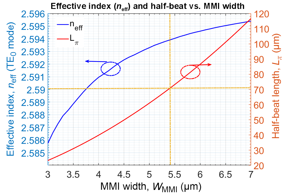
Fig. 2 showed the effective index and the half-beat length of the MMI region as a function of the MMI width (WMMI) at an operating wavelength of 1550 nm, using the 3D-BPM simulation method. For the chosen width WMMI = 5.4 μm, the effective index, neff, was approximately 2.59. Therefore, substituting this into (1) and (2), Lπ ≈ 70.8 μm was obtained. Next, the authors examined the optical transmission characteristics depending on the MMI length from 20 μm to 120 μm, which covered the entire range of MMI lengths calculated theoretically, with a resolution of 0.5 μm, encompassing the range from Lπ / 2 to 3Lπ / 2. In the simulation, the optical field at a wavelength of 1550 nm under TE polarization was injected into the proposed structure through the input port assigned as Port1.
Fig. 2.3D-BPM simulations for the MMI coupler: the effective
index, neff, and the half-beat length, Lπ are functions of
the width of the MMI waveguide.
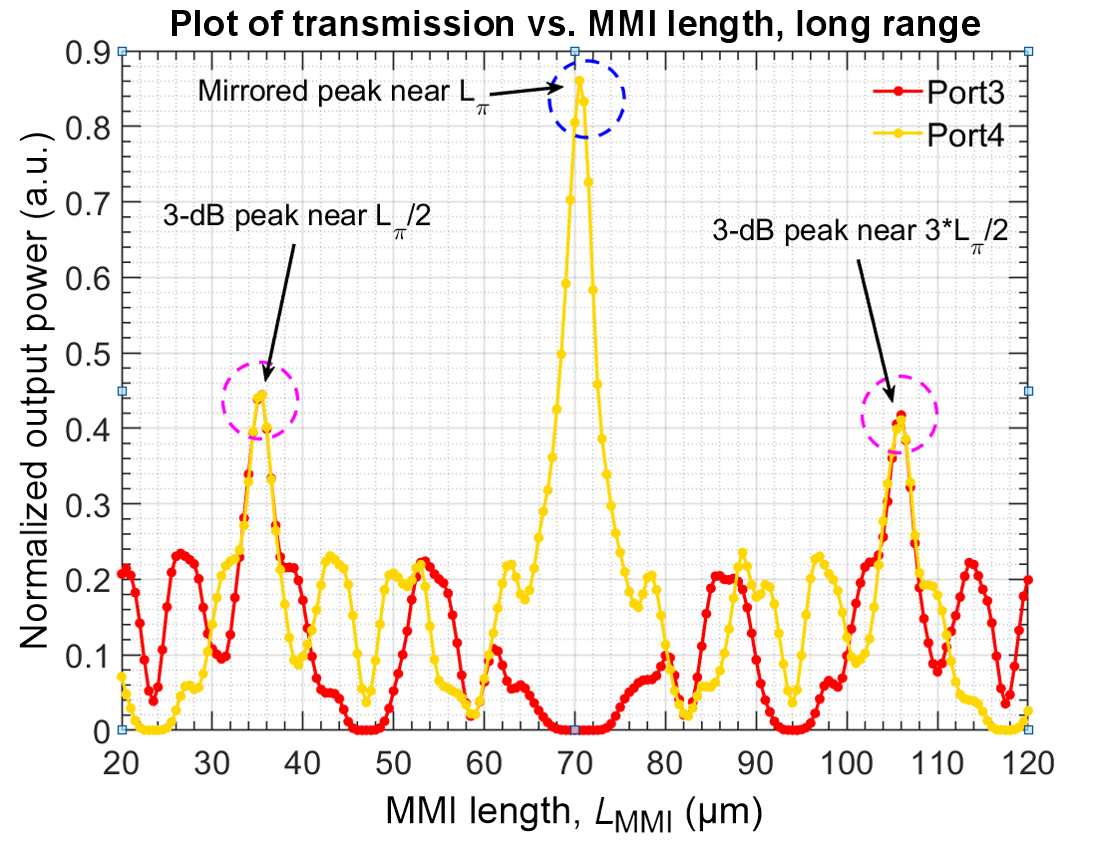
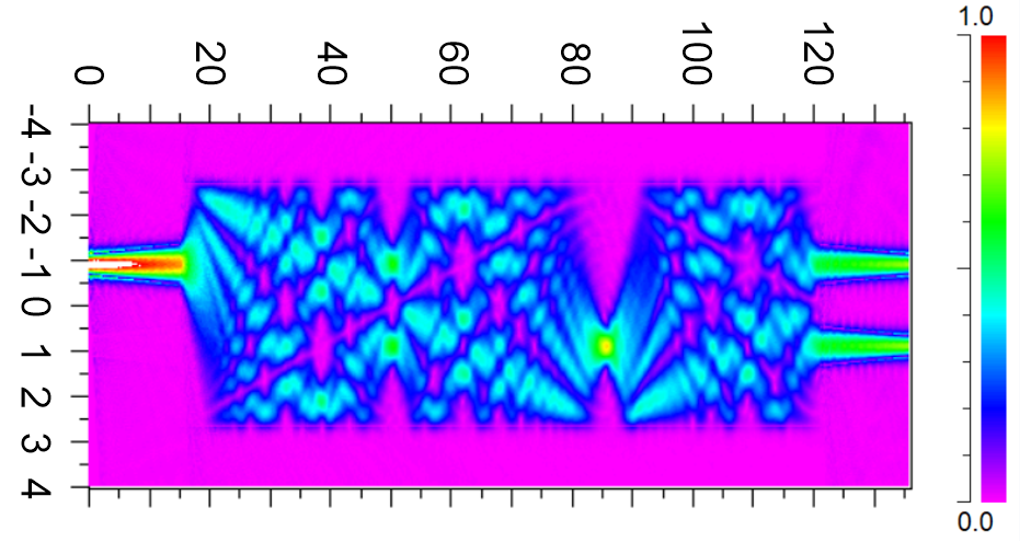
To determine the optimal length of the device, the length of the multimode region (LMMI) was initially varied from 20 μm to 120 μm, covering the entire range of MMI lengths mentioned. The plot revealed two regions where the outputs are equal, indicating an ideal 50:50 splitting ratio. These regions spanned approximately from 30 μm to 40 μm and from 100 μm to 110 μm. Additionally, there was a region near 71 μm showing a mirrored image of the input field. For a more detailed analysis of the two potential length ranges, Fig. 3(b) illustrates the electric field pattern under a contour map when the MMI length is 106.2 μm. It can be observed that there are three clearly observed images, confirming the wavelength-dependent results from Fig. 3(a). Therefore, in this design, the authors chose the MMI coupler with its length within the range of 30–40 μm, near the length of Lπ / 2.
Fig. 3. (a) Normalized output power transmission characteristic
dependence on the MMI length is swept in the range from
20 μm to 120 μm and (b) electric field pattern of the
MMI coupler at a length of 106.2 μm.
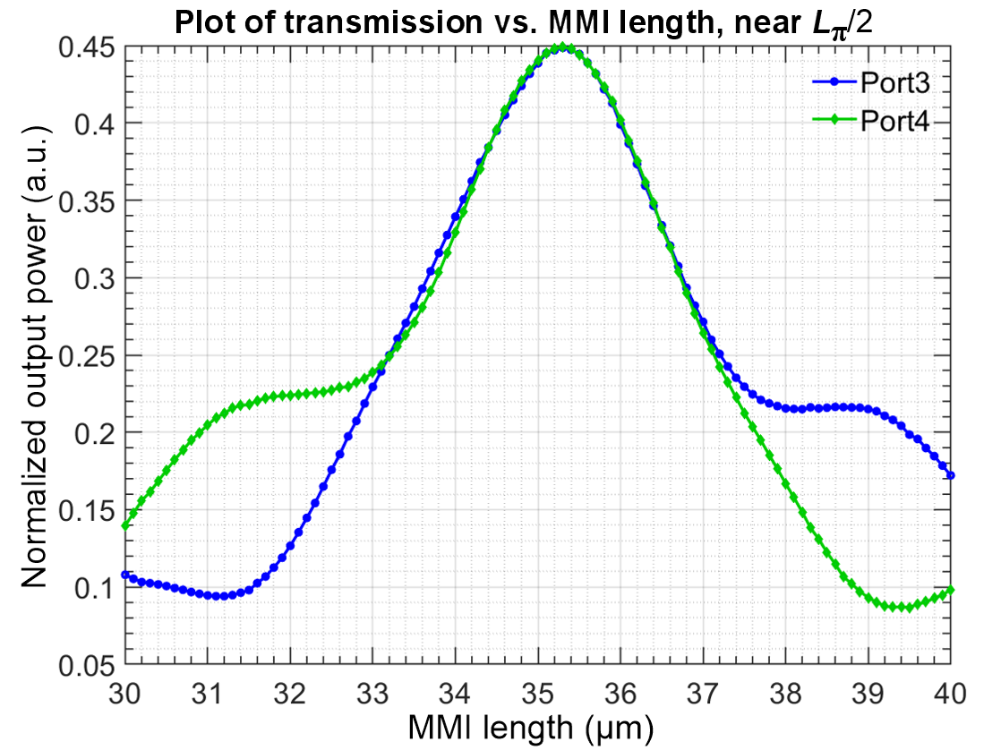
To investigate further and determine a more accurate value for the MMI length, the authors configured the length to the respective ideal value by sweeping the MMI length from 30 μm to 40 μm with a 0.1 μm resolution. Fig. 4 illustrated the transmission characteristics of the two output ports, Port3 and Port4, as a function of the MMI coupler length near Lπ / 2. The results showed that the two curves reached a transmission peak (approximately 45%) at a length of approximately LMMI = 35.3 μm. Notably, within the range of 33.2–37.4 μm, the characteristics of the two output ports were nearly identical, forming a parabolic shape symmetrical about the line through the point 35.4 μm, with values ranging from 25% to 45%. Thus, it could be seen that the 3-dB bandwidth around the peak value extended over a wider range of ± 2.1 μm around a central value of 35.3 μm. In this design, the authors selected the value LMMI = 35.4 μm because, at this value, the two curves intersected, indicating an ideal 50:50 splitting ratio.
Fig. 4.High-resolution swept transmission spectra of outputs
depend on the length of the MMI region simulated by the
3D-BPM method at an operation wavelength of
1550 nm.
Device performance characterization
Fig. 5 displays the electric field pattern of the device (top-view) with an MMI region length of 35.4 μm. As demonstrated in the electric field evolution diagram, the incident light wave has already been equally divided. Especially, the main section of the power splitter, based on the designated 2 × 2 MMI coupler, can be laid out on a foot-print of 6 μm × 65 μm, demonstrating its compactness for large-scale integration.
Fig. 5.3D-BPM simulation of the electric field distribution
under TE mode of the designed power splitter at an MMI
length of 35.4 μm
To benchmark the device performances, the authors also worked out the EL of the device through each output port, which can be determined using the formula [31]:
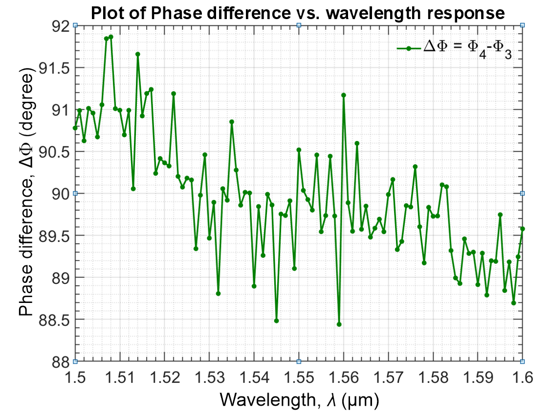
where Pout and Pin correspond to the output and input powers, respectively. The constant quantity of 3 dB in (3) implies that the input light wave is divided into two output ports with a splitting ratio of 50:50. Moreover, a 3-dB power splitter for applications in advanced photonic circuits, such as optical switches and optical modulators, should maintain the phase difference between the two output ports (ΔΦ = Φ4 − Φ3) as a constant, emphasizing minimal fluctuation of the phase difference. As can be seen from Fig. 6(a), the excess losses (ELs) of the two output ports are consistently similar and closely follow smooth curves vs. wavelength response over a broad range of 100 nm from 1500 nm to 1600 nm. Additionally, the minimum ELs of the device are 0.48 dB at the wavelength of 1546 nm and the maximum ELs are 2.7 dB at the wavelength of 1600 nm, demonstrating the ultra-low loss of the device over a broad wavelength range. At a central wavelength of 1550 nm, EL is 0.5 dB. Simulation results show that the phase difference varies very slightly, from 88.4° to 91.9°, resulting in a relative phase difference that does not exceed 2% around the desired phase difference value of 90° over a broad spectrum up to 100 nm, as seen in Fig. 6(b). It is evident that the 35.4 μm-length device exhibits significant performance in terms of EL and phase difference, making it an appealing choice for a variety of sophisticated functional photonic integrated circuits.
Fig. 6. Optical performance wavelength-dependency of the
designed 3-dB power splitter based on the RI-MMI
coupler in 100-nm spectra for two output ports: (a) EL
and (b) phase difference.
A photonic device with a transmission spectrum like a filter, modulator, or switch requires a smooth spectral response to indicate stable and consistent operation over a wide frequency range. Conversely, amplitude and phase fluctuations or strong ripples in the transmission spectrum can lead to signal distortion, system noise, increased error vector magnitude (EVM), and operational instability. The authors will assess the impact of amplitude fluctuations of the proposed 3-dB device by examining the residual deviation of the output characteristics around a smoothed function of the transmission spectra of the two output ports, Port3 and Port4, respectively denoted by the residual measurement values Δ3, Δ4. The residual deviation in the transmission characteristics of an output port is defined as follows:
where Pout (discrete) is the power measured by a power meter or simulated data, Psmooth is the power obtained by the smoothed function value of the spectral curve. Fig. 7 depicts the residual deviation plotted against wavelength response within the range of 1500–1600 nm, presented on a decibel scale. On the left axis, one will find the residual values at Port3, indicated by the blue curve, while the residual values at Port4, represented by the red curve, are displayed on the right axis. The findings reveal that both output ports exhibit negligible residual, with the maximum residual peaking at −18 dB and the minimum value dropping to −49 dB.
Fig. 7.EL residual dependence on the wavelength response in
an ultrawide range of 100 nm from 1500 nm to 1600 nm.
Simulation data from two output ports are measured and
smoothed. The blue and red lines represent the residual
values of Port3 (Δ3) and Port4 (Δ4) at an MMI length of
34.5 μm, respectively.
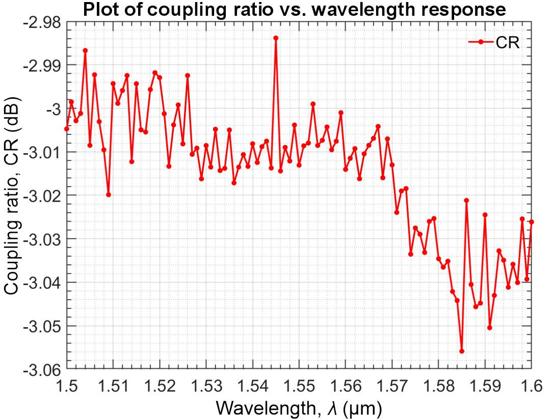
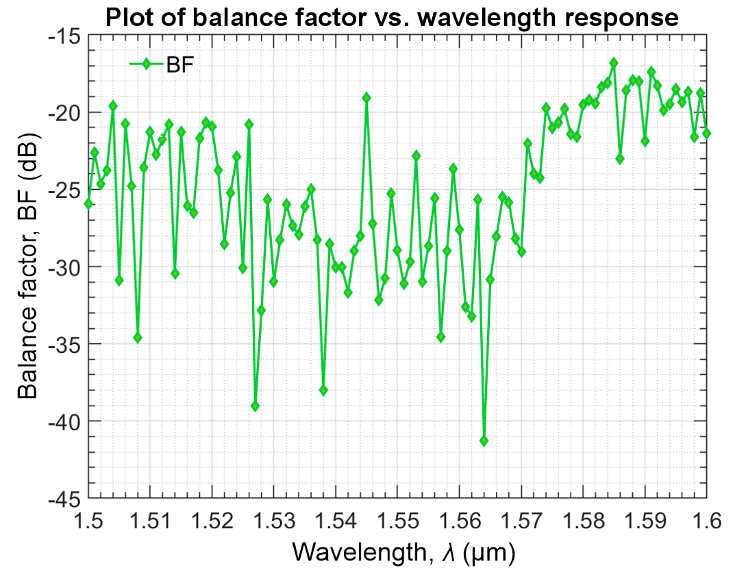
Subsequently, the authors employed standardized equations to ascertain the coupling ratio (CR) and the balance factor (BF) of the devices, facilitating the identification of those achieving optimal 50:50 power splitting. CR and BF are described as follows:
where Pout3 and Pout4 are corresponding to the output power of the Port3 and Port4, respectively. The CR represents the percentage ratio of power transferred from the input port to each output port. It indicates the percentage of input power transferred to each output port compared to the total input power. CR is commonly used to measure the power distribution in power distribution devices such as optical splitters, amplifiers, and filters. Meanwhile, the balance factor measures the difference between the power at two output ports and indicates the balance level of the two output ports. BF is often used to evaluate the performance and uniformity in power distribution or connection between pairs of ports in devices such as splitters or couplers. Fig. 8(a) shows the simulation results of the coupling coefficient CR as a function of wavelength dependence. The results show that the coupling coefficient varies slightly in the range from −2.98 dB to −3.05 dB, around the central point of 3 dB, over a wide spectral range up to 100 nm. Fig. 8(b) shows the simulation results of the BF according to the wavelength response from 1500 nm to 1600 nm. The simulation results show that the balance of the two ports due to the limited interference characteristics of the device is very high because, on the decibel scale, BF is small, fluctuating only from the highest value of −17 dB to the lowest value of −41 dB. At the centre wavelength of 1550 nm, the balance level is very high because BF = −31 dB (less than 0.1%).
Fig. 8. Wavelength response characteristics of the proposed
power splitter ranging from 1500 nm to 1600 nm: (a) CR
and (b) BF.
Fabrication tolerance in photonic devices based on waveguides is of great importance and relates to various aspects of the design and manufacturing process. The smaller the tolerance, the higher the precision required in the fabrication process, consequently increasing production costs. Fabrication tolerance reflects the capability of the available fabrication process. CMOS process technologies, such as photolithography and etching, have limitations in accuracy, so devices must be designed to accommodate these limits. Additionally, a reasonable fabrication tolerance design helps ensure high repeatability of fabricated devices, meaning different devices produced from the same process will have equivalent performance. This is crucial for mass production and commercialization. Fig. 4 shows that the 3-dB width tolerance is very large, up to ± 2.1 μm. Fig. 9 describes the survey of EL and phase difference characteristics depending on the height tolerance of the SOI wafer, with a tolerance of Δh = ± 10 nm. The results in Fig. 9(a) show that the EL fluctuates within a small range of −0.46 dB to −0.84 dB, while the results in Fig. 9(b) indicate an extremely small phase difference variation, ranging from 89.7° to 91.4°, which means a deviation of no more than 1.5% from the desired phase difference value of 90° within a relatively high tolerance of ± 10 nm. To the best of the authors’ knowledge, such a tolerance can currently be achieved using DUV-193 nm photolithography and plasma etching processes.
Fig. 9. Fabrication tolerances on the height of a silicon core
layer of the proposed device for two output ports: (a) EL
and (b) phase difference.
Conclusions
In conclusion, the authors have utilized an optimized design featuring a silicon 2 × 2 MMI-based 3-dB optical power splitter, employing the restricted interference regime to reduce device length. Numerical simulations conducted using the 3D-BPM method identified the optimal MMI length as 35.4 μm. Numerical simulation results yielded an excellent optical performance for the designed 2 × 2 RI‑MMI coupler, with low EL (< 2.7 dB), small relative phase difference (< 2%), negligible residual (< −18 dB), excellent CR (−0.09 dB to 0.05 dB), and high BF (< −17 dB) across a wide range of 100 nm (1500 nm–1600 nm), including 30 nm of the S-band (1500–1530 nm), the entire C-band (1530 nm–1565 nm), and 35 nm of the L‑band (1565 nm–1600 nm). In addition, the designed device demonstrated large geometry tolerances with ± 2.1‑μm width tolerance and ± 10-nm height tolerance. Furthermore, the major section of the proposed power splitter, based on the restricted interference 2 × 2 MMI coupler, could be accommodated within a compact foot-print of 6 μm × 65 μm. These outstanding characteristics position the proposed device as a promising candidate for the development of very large-scale photonic integrated circuits and photonic neural networks in ultrawideband telecom applications.
References
Wang, S. & Dai, D. Polarization-insensitive 2 × 2 thermo-optic Mach–Zehnder switch on silicon. Opt. Lett. 43, 2531–2534 (2018). https://doi.org/10.1364/OL.43.002531
Luo, A.-P., Luo, Z.-C. & Xu, W.-C. Multiwavelength switchable erbium-doped fiber ring laser with a PBS-based Mach-Zehnder comb filter. IEEE Photon. J. 3, 197–202 (2011). https://doi.org/10.1109/JPHOT.2011.2120601
Goi, K. et al., 128Gb/s DP-QPSK Silicon Modulator Module Integrated with Driver Amplifiers. in 2014 The European Conference on Optical Communication (ECOC) 3–5 (IEEE, 2014). https://doi.org/10.1109/ECOC.2014.6964199
Velha, P. et al. Wide-band polarization controller for Si photonic integrated circuits. Opt. Lett. 41, 5656–5659 (2016). https://doi.org/10.1364/ol.41.005656
Xu, X., Zhu, L., Zhuang, W., Lu, L. & Yuan, P. A convolution neural network implemented by three 3 × 3 photonic integrated reconfigurable linear processors. Photonics 9, 80 (2022). https://doi.org/10.3390/photonics9020080
Yamada, H., Chu, T., Ishida, S. & Arakawa, Y. Si photonic wire waveguide devices. IEEE J. Sel. Top. Quantum Electron. E90-C, 59–64 (2007). https://doi.org/10.1093/ietele/e90-c.1.59
Sun, L., Zhang, Y., He, Y., Wang, H. & Su, Y. Subwavelength structured silicon waveguides and photonic devices. Nanophotonics 9, 1321–1340 (2020). https://doi.org/10.1515/nanoph-2020-0070
Chung, K. K., Chan, H. P. & Chu, P. L. A 1 × 4 polarization and wavelength independent optical power splitter based on a novel wide-angle low-loss Y-junction. Opt. Commun. 267, 367–372 (2006). https://doi.org/10.1016/j.optcom.2006.06.048
Tao, S. H. et al. Cascade wide-angle Y-junction 1 × 16 optical power splitter based on silicon wire waveguides on silicon-on-insulator. Opt. Express 16, 21456 (2008). https://doi.org/10.1364/OE.16.021456
Zhang, Y. et al. A compact and low loss Y-junction for submicron silicon waveguide. Opt. Express 21, 1310–13–16 (2013). https://doi.org/10.1364/oe.21.001310
Yun, H., Chrostowski, L. & Jaeger, N. A. F. Ultra-broadband 2 × 2 adiabatic 3 dB coupler using subwavelength-grating-assisted silicon-on-insulator strip waveguides. Opt. Lett. 43, 1935–1938 (2018). https://doi.org/10.1364/ol.43.001935
Nguyen, V. H., Kim, I. K. & Seok, T. J. Low-loss and broadband silicon photonic 3-db power splitter with enhanced coupling of shallow-etched rib waveguides. Appl. Sci. 10, 4507 (2020). https://doi.org/10.3390/app10134507
Luo, Y., Yu, Y., Ye, M., Sun, C. & Zhang, X. Integrated dual-mode 3 dB power coupler based on tapered directional coupler. Sci. Rep. 6, 23516 (2016). https://doi.org/10.1038/srep23516
Wang, Z. et al. Ultra-broadband 3 dB power splitter from 1.55 to 2 µm wave band. Opt. Lett. 46, 4232–4235 (2021). https://doi.org/10.1364/ol.430827
Liu, Z., Dong, Y., Xu, Y., Zhang, B. & Ni, Y. Low loss and ultra- broadband design of an integrated 3 dB power splitter centered at 2 µm. Appl. Opt. 63, 662–667 (2024). https://doi.org/10.1364/ao.510814
Lu, M. et al. Compact and broadband 2 × 2 3 dB optical power splitter based on bricked subwavelength gratings. Opt. Commun. 561, 130539 (2024).https://doi.org/10.1016/j.optcom.2024.130539
Xu, J., Liu, Y., Guo, X., Song, Q. & Xu, K. Inverse design of a dual-mode 3-dB optical power splitter with a 445 nm bandwidth. Opt. Express 30, 26266–26274 (2022). https://doi.org/10.1364/oe.463274
Yang, S. et al. Photonics inverse-designed compact dual-mode 3 dB power splitter for on-chip MDM systems. Opt. Laser Technol. 170, 110281 (2024). https://doi.org/10.1016/j.optlastec.2023.110281
Zheng, L. et al. UV-LED projection photolithography for high- resolution functional photonic components. Microsyst. Nanoeng. 7, 64 (2021). https://doi.org/10.1038/s41378-021-00286-7
Farrokhi Chaykandi, Z., Bahrami, A. & Mohammadnejad, S. MMI- based all-optical multi-input XOR and XNOR logic gates using nonlinear directional coupler. Opt. Quant. Electron. 47, 3477–3489 (2015). https://doi.org/10.1007/s11082-015-0224-0
Anagha, E. G. & Jeyachitra, R. K. Review on all-optical logic gates: design techniques and classifications – heading toward high- speed optical integrated circuits. Opt. Eng. 61, 060902 (2022). https://doi.org/10.1117/1.oe.61.6.060902
Pal, S. & Gupta, S. Proposal and analysis of a silicon MMI coupler- based electronically controllable photonic switch. IEEE J. Sel. Top. Quantum Electron. 22, 141–154 (2016). https://doi.org/10.1109/JSTQE.2016.2545239
Deng, Q., Liu, L., Li, X. & Zhou, Z. Arbitrary-ratio 1 × 2 power splitter based on asymmetric multimode interference. Opt. Lett. 39, 5590–5593 (2014). https://doi.org/10.1364/ol.39.005590
Li, Z. et al. Ultra-compact low-loss variable-ratio 1 × 2 power splitter with ultra-low phase deviation based on asymmetric ladder-shaped multimode interference coupler. Opt. Express 28, 34137–34146 (2020). https://doi.org/10.1364/oe.405449
Yi, Q. et al. Silicon MMI-based power splitter for multi-band operation at the 1.55 and 2 µm wave bands. Opt. Lett. 48, 1335–1338 (2023). https://doi.org/10.1364/ol.486428
Luo, Y., Yu, Y., Ye, M., Sun, C. & Zhang, X. Integrated dual- mode 3 dB power coupler based on tapered directional coupler. Sci.Rep. 6, 23516 (2016). https://doi.org/10.1038/srep23516
Zollner, S. et al. Thin-film metrology of silicon-on-insulator materials. Appl. Phys. Lett. 76, 46–48 (2000). https://doi.org/10.1063/1.125651
Xu, D.-X. et al. Empirical model for the temperature dependence of silicon refractive index from O to C band based on waveguide measurements. Opt. Express 27, 27229–27241 (2019). https://doi.org/10.1364/oe.27.027229
Dwivedi, S. et al. Experimental extraction of effective refractive index and thermo-optic coefficients of silicon-on-insulator wave- guides using interferometers. J. Light. Technol. 33, 4471–4477 (2015). https://doi.org/10.1109/JLT.2015.2476603
Soldano, L. B. & Pennings, E. C. M. Optical multi-mode interference devices based on self-imaging: Principles and applications. J. Light.Technol. 13, 615–627 (1995). https://doi.org/10.1109/50.372474
Jiao, Y., Shi, Y., Dai, D. & He, S. Accurate and efficient simulation for silicon-nanowire-based multimode interference couplers with a 3D finite-element mode-propagation analysis. J. Opt. Soc. Am. B 27, 1813–1818 (2010). https://doi.org/10.1364/josab.27.001813
Yamauchi, J., Shibayama, J., Saito, O., Uchiyama, O. & Nakano,