The paper analyses the performance of avalanche barrier infrared detectors based on the bulk InAsSb ternary compound of AIII-BV materials, lattice-matched to the GaSb substrate for a long-wavelength range operating at thermoelectric cooling conditions. A ternary Al0.2As0.8Sb barrier was assumed. Particular attention was paid to the influence of avalanche multiplication layer parameters on the device current-voltage characteristics and current gain. Numerical simulations were performed using a SimuApsys software for the npBp InAsSb detector operating at the temperature achieved by a two-stage thermoelectric cooler (TE), T = 230 K. Based on the analysis of the literature data of the avalanche ionisation coefficient and the density of the band-to-band tunnelling currents, the conditions in which the Zener effect does not reduce the multiplication process were determined. The highest gain can be achieved with a low level of multiplication layer doping and a lower molar composition of antimony compared to the absorber composition (larger band gap energy). The gain also increases with the multiplication of layer thickness. The paper discusses the design of the long-wavelength avalanche detectors based on InAsSb with an optimised multiplication process.
Introduction
Indium arsenide antimonide is a bulk semiconductor with a low band gap energy. It is widely used as a base material in the construction of optoelectronic devices in the medium-wave infrared (MWIR) and long-wave infrared (LWIR) ranges [1, 2]. InAsSb infrared (IR) detectors have garnered considerable attention for many years due to their high quantum efficiency and desirable electrical and optical properties [3]. In conventional junction detectors operating at high operating temperature (HOT) conditions, the dark current results from generation-recombination processes via Shockley-Read-Hall (SRH) centres, Auger process, and band-to-band tunnelling (BTBT) [3]. To improve detector sensitivity, avalanche photodiodes (APDs) can be used. These detectors also exhibit high dark current due to the carrier recombination effect [4]. Therefore, the use of an additional wide energy gap barrier between the contact and the absorbing (active) layers allows for extending the operating temperature and dark current suppression [5]. Among the proposed barrier detectors, nBn devices have found the widest application [6–10].
In recent years, a significant progress has been made in the development of LWIR APDs, covering materials based on mercury cadmium telluride (HgCdTe) and AIII-BV alloys, including type-II superlattices (T2SLs) [11]. The feasibility of fabricating InAs, InSb, InAsSb, or InAlSb-based APDs has also been reported [12–15]. InAs/InAsSb T2SLs have emerged as an alternative to bulk InAsSb and HgCdTe materials in recent years. The properties of IR detectors made of AIII-BV compounds are comparable to those of HgCdTe detectors. However, AIII-BV compounds are characterised by shorter SRH recombination lifetimes than HgCdTe, which allows for increasing the operating temperature of these detectors [16].
This paper proposes an avalanche barrier IR detector based on a ternary InAsSb compound lattice-matched to a GaSb substrate for the LWIR range operating at 230 K. The npBp APD was designed to be backside-illuminated in a mesa-type structure. The main objective of the research was to analyse the effect of the avalanche multiplication layer parameters on the detector current-voltage charac-teristics and current gain. The multiplication process and the influence of molar composition, doping, and multiplica-tion layer thickness on the APD performance were investigated. The research that was conducted indicates the possibility of constructing InAsSb avalanche detectors for the LWIR operating range. InAsSb detectors on GaSb substrate were presented in [17], but there is no data on avalanche multiplication.
Avalanche photodiode (APD) design and numerical simulation method
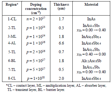
The avalanche barrier IR detectors were based on InAs1-xSbx lattice-matched to the GaSb substrate. The structure consisted of a lower contact layer (CL) made of InAs, a multiplication layer (ML), and an absorber layer (AL) made of InAs0.6Sb0.4 located between transient layers (TLs) made of InAs1-xSbx with a molar composition gradient xSb from 0.0 to 0.4, an Al0.2As0.8Sb barrier with another TL and an upper CL. The schematic structure and the energy band diagram of this detector are shown in Fig. 1. The details regarding the thickness and doping of indivi-dual layers are presented in Table 1. Numerical simulations were carried out using the SimuApsys software (Crosslight) [18]. The calculations assumed the Auger recombination coefficient for electrons and holes at the level of 5 × 10-39 [m6/s], the SRH recombination lifetime of 1 μs, and the radiative recombination coefficient τR = 8.9 1017 [m3/s] at T = 230 K. The detector was illuminated from the lower CL with a radiation of an 8.0 μm wavelength and a power of 1000 W/m2. The input data of the ternary materials [band gap energy, valence band offset, effective carrier (electron and hole) mass, carrier mobility], InAs1-xSbx and Al1-xAsxSb, were determined according to Vegard’s law, taking into account the nonlinear bowing parameters [19].
Fig. 1.Structure and band gap energy diagram vs. APD profile
(unbiased condition).
In the studied structure, practically the entire potential drops in the TL and the ML. The potential barrier in the conduction band established in the TL disappears when the junction is reverse-biased and does not affect the shape of the I-V characteristics.
The effect of avalanche ionisation was taken into account in the calculations based on the Chynoweth model [20], assuming electron and hole ionisation coefficients of the form:
\(
\alpha_e=a_e \cdot e^{\frac{-b_e}{E}}
\) (1)
\(
\alpha_h=a_h \cdot e^{\frac{-b_h}{E}}
\) (2)
where E is the electric field in the multiplication region, ae,h and be,h are the material parameters of the multiplication process. Literature data indicate a significant scatter in the adopted values of the ionisation coefficients ae,h and be,h, with most works devoted to AIII-BV materials focusing mainly on InAs and T2SLs, such as InAs/InAsSb. The authors also quite often analyse ternary and quaternary compounds containing aluminium. The selection of para-meters, as presented in the authors’ work, was based primarily on the analysis of literature data for the materials mentioned above. The electron multiplication coefficient for InAsSb was determined based on the data for InAs material, selecting the material parameters of the multipli-cation process, ae,h and be,h in such a way as to obtain the ionisation level presented in [21]. In this work, two sets of material parameters of the multiplication process were analysed:
Fig. 2 shows the dependence of the impact ionisation coefficients of electrons and holes on the inverse of the electric field for those sets. At the typical electric fields (3 × 10⁴ V/cm), the carriers ionisation coefficients for both sets of parameters are comparable, while for fields lower than 3 × 10⁴ V/cm, ionisation Set#1 predominates, and for E > 3 × 10⁴ V/cm, ionisation Set#2 is higher.
The multiplication factor (avalanche gain M) was determined based on (3). It is the ratio between the photo-current and current at a given voltage to the photocurrent at zero polarization.
Fig. 2.Electron and hole impact ionisation coefficients vs.
inverse of the electric field for two sets of material
parameters (multiplication process #1 and #2).
\(
M(V)=\frac{J_{p h}(V)}{J_{p h}(V=0)}
\) (3)
The APD detector noise is related to the thermally generated dark currents resulting from the fluctuations of charge carriers generated by photons and is described by the expression:
\(
I_s^2=2 q I_{\mathrm{ph}} M^2 F(M)
\) (4)
where M is the avalanche photo gain, F(M) is the excess noise factor, and Iph is the photocurrent. Excess noise is a consequence of statistical fluctuation in the multiplication process. In the case of electron injection only, the excess noise factor F(M) is defined by [13]:
By reducing the dark current and excess noise of the detector, a high internal gain can be achieved over a wide bandwidth.
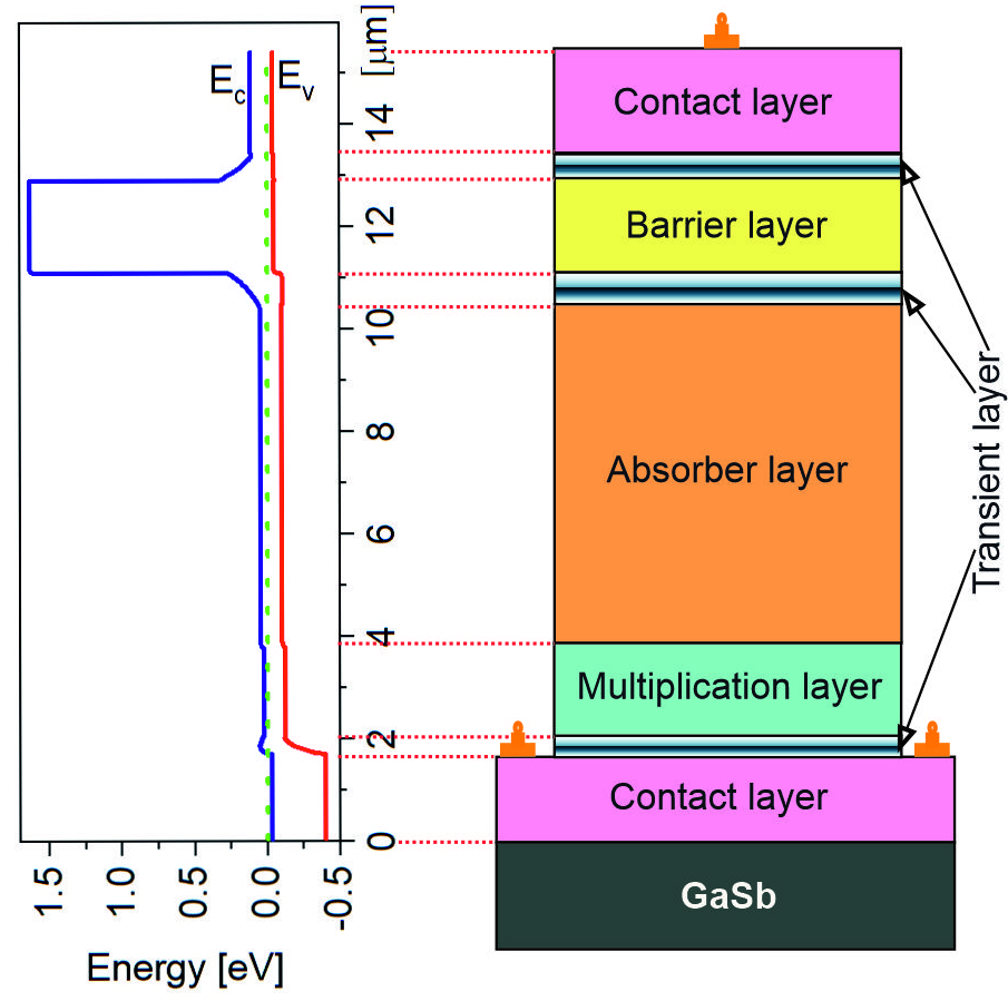
A significant problem in the case of narrow-band APD detectors in the LWIR range is the occurrence of Zener-type BTBT currents, which influence the avalanche multiplication process. Fig. 3 shows the impact of the carrier ionisation rate on the APD I-V characteristics. At a high ionisation rate for low electric field strengths (Set #1), the breakdown voltage associated with the multiplication effect is much smaller than the Zener breakdown voltage, and the tunnelling effect does not affect the APD detector parameters. Fig. 3(a) shows the I-V characteristics without taking into account Zener ionisation and tunnelling, only assuming Zener tunnelling and impact ionisation, and Zener tunnelling. It can be seen that the influence of the tunnelling effect appears only for reverse voltages above 4 V, while the impact ionisation process occurs already at voltages above 100 mV.
Fig. 3. I-V characteristics of the APD detector with and without
the Zener current for impact ionisation parameters #1 (a)
and #2 (b) at T = 230 K.
However, at a low ionisation rate for low electric field strengths (Set #2), the ionisation multiplication “breakdown” voltage is approximately 18 V, and assuming the tunnelling effect causes its shift to a voltage of about 2 V [Fig. 3(b)].
The comparison of the impact ionisation rate on the I-V characteristics, the gain and excess noise factor of the APD detector for both sets of ionisation parameters, taking into account the Zener tunnelling currents, is shown in Fig. 4.
Fig. 4. Influence of the impact ionisation rate on the I-V
characteristics (a) and excess noise factor vs. the
avalanche multiplication gain (b) for the APD detector at
230 K for set #1 and #2.
The avalanche multiplication factor M (gain) and excess noise factor were determined according to (3) and (5), respectively [Fig. 4(b)]. The impact ionisation breakdown voltage for the ionisation parameter of Set#2 is three times higher than for the parameter of Set#1. In contrast, the dark current density at a given voltage is lower. Although for impact ionisation parameters marked with the symbol Set#1, it is possible to obtain impact ionisation amplification of more than 20 times, the case of Set#2 appears to be closer to the experimental data of the APD for the LWIR range. Therefore, these values of the impact ionisation rate parameters were adopted in subsequent calculations [22]. In the case of Set#2, the excess noise factor is much smaller than in the case of Set#1 parameters
Results and discussion
Initially, the distribution of electric field intensity was compared with the impact ionisation rate and the carrier concentration distribution in the analysed APD structure. Fig. 5(a) shows the distribution of electric field and carrier ionisation rate, and Fig. 5(b) shows the carrier concentration distribution without bias (n0, p0) and with the voltage U = −6V (n, p) for the APD detector at a tempera-ture of 230 K. It can be seen that almost the entire electric field is deposited in the ML and the TL. The most significant carrier ionisation occurs in the TL region, indicating that it is an electron ionisation process, which is consistent with the adopted values of ionisation parameters. An apparent decrease in the concentration of electrons and holes is observed in the ML region.
Fig. 5. Distribution of the electric field (blue line) and impact
ionisation rates (red line) (a) and carrier concentration
distribution without bias (n0, p0) and at voltage U = −6V
(n, p) (b) for the APD detector at 230 K.
The influence of the AL doping level on the I-V characteristics and the avalanche multiplication gain of the APD detector was analysed. Optionally, the AL was doped to p-type at the level of 1 × 1016 cm-6. However, the AL doping of 2 × 1016 cm-6 was assumed to analyse the influence of the ML doping. Fig. 6(a) shows the dark current density as a function of the reverse bias for the AL for three selected doping levels: 5 × 1015 cm-6, 1 × 1016 cm-6, and 2 × 1016 cm-6. Influence of the AL doping on the avalanche multiplication gain is shown in Fig. 6(b). Lowering the doping level of the AL causes a decrease in the dark current density in the reverse direction. Still, it does not affect the avalanche multiplication gain factor [see Fig. 6(b)]. For the three analysed AL doping levels, the gain reaches practically the same values.
Fig. 6. Influence of the AL doping level on the I-V characteristics
(a) and avalanche multiplication gain (b) for the
APD detector at 230 K. (ML: xSb = 0.30, p = 1 × 1015 cm-6,
d = 1.8 μm).
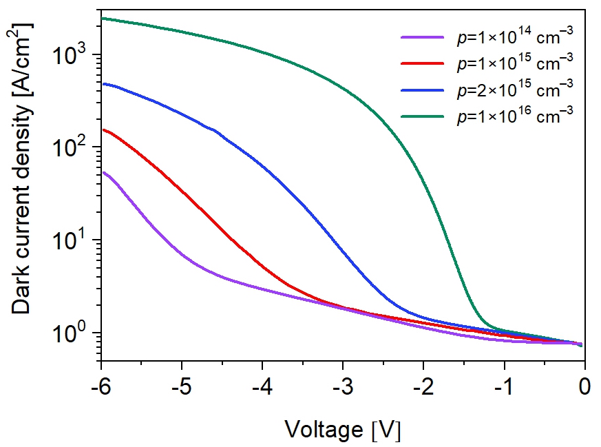
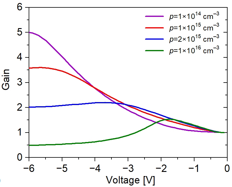
In APD structures, the parameters of the ML play an important role. Fig. 7 shows the effect of the ML layer doping level on the I-V characteristics in the reverse direction. Increasing the ML doping level causes an increase in dark currents and a shift of the “avalanche breakdown voltage” towards lower voltages. The current gain increases with the ML doping level, and its maximum value shifts towards higher voltages [Fig. 7(b)]. These changes are caused by the change in the electric field distribution, which significantly affects the impact ionisation rate.
Fig. 7.Dark I-V characteristics (a) and avalanche multiplication
gain (b) for four ML doping levels: 1 × 1014 cm-6,
1 × 1015 cm-6, 2 × 1015 cm-6, 1 × 1016 cm-6, (AL:
p = 1 × 1015 cm-6, ML: d = 1.8 μm, AL, ML: xSb = 0.30).
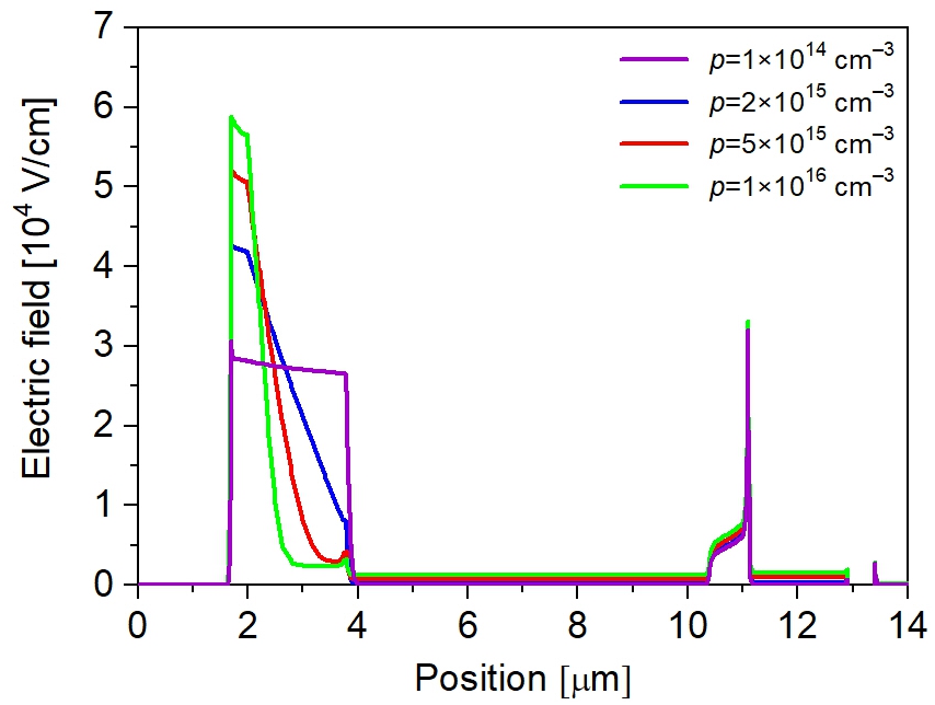
The voltage mainly drops in the TL and ML, with some portion entering the AL. Fig. 8 shows the distribution of the electric field intensity as a function of the thickness of the tested structure for the above-mentioned doping levels of the ML. Increasing the doping level in the ML layer causes a decrease in the electric field intensity in the ML and a significant increase in the transient region [ Fig. 8(a)], and thus an increase in the impact ionisation rate illustrated in Fig. 8(b). Ionisation occurs mainly in the TL and the part of the ML located near it.
Fig. 8.Distribution of electric field intensity (a) and impact
ionisation rate (b) for four ML doping levels: 1 × 1014 cm-6,
2 × 1015 cm-6, 5 × 1015 cm-6, 1 × 1016 cm-6, (AL:
p = 1 × 1015 cm-6, ML: d = 1.8 μm, AL, ML: xSb = 0.30).
The electric field intensity in the ML can also be increased by changing its molar composition (antimony content in ternary InAs1-xSbx ). With a decrease of the Sb content in the absorber (xSb = 0.40), the ML energy gap increases, and thus its electrical conductivity decreases, and a larger electric field is deposited in the ML. Fig. 9 shows the effect of the molar composition of the ML (xSb = 0.40; xSb = 0.38; xSb = 0.35 and xSb = 0.30) on the dark current level [Fig. 9(a)] and gain [Fig. 9(b)] for the tested APD detector at a temperature of 230 K.
Fig. 9.Influence of the stoichiometric composition of the ML
layer on the I-V characteristics (a) and the avalanche
multiplication gain (b) for the APD detector at 230 K (AL:
p = 1 × 1015 cm-6, ML: p = 1 × 1015 cm-6, d = 1.8 μm).
Increasing the ML band gap width causes a decrease in the dark current and an increase in the avalanche multi-plication gain to 20. The “avalanche breakdown voltage” also increases.
The next step of the theoretical research was to analyse the effect of the ML thickness on the I-V characteristics. Fig. 10(a) shows the I-V characteristics for three selected thicknesses of the ML: 1.8 μm, 1.2 μm, and 0.6 μm. Reducing the thickness of the ML causes an increase in the dark current density and the occurrence of an avalanche amplification effect in the tested structure at lower reverse bias. For voltages below the breakdown value, the dark current density remains constant. The avalanche multipli-cation gain vs. bias for selected ML thicknesses was presented in Fig. 10(b). The avalanche multiplication gain reaches its maximum value near the breakdown voltage and then decreases rapidly. However, a higher current gain is obtained with thicker MLs, but at higher reverse bias.
Fig. 10.Dark current density (a) and the avalanche multiplication
gain (b) vs. voltage for selected ML thicknesses (for
d = 1.8 μm, d = 1.2 μm, and d = 0.6 μm) at 230 K (AL:
p = 1 × 1015 cm-6, ML: p = 1 × 1015 cm-6, xSb = 0.30).
The conducted analysis of the influence of the absorber and MLs parameters on the avalanche multiplication coefficient of APD barrier IR detectors with InAs1-xSbx absorber showed a slight influence of the AL doping level on the gain of the tested detector. At the same time, the molar composition and the ML thickness are essential in terms of the impact ionisation process.
Comparison of the HgCdTe and InAsSb APD detectors
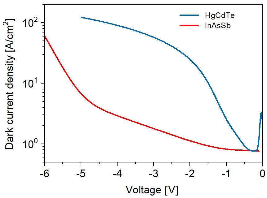
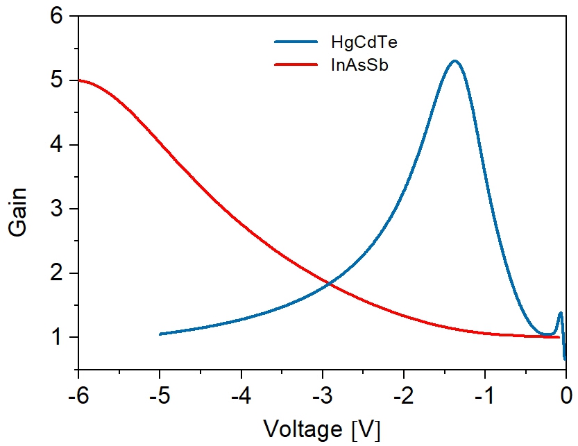
The performance of LWIR HgCdTe APDs for HOT conditions was analysed in [23]. The HgCdTe detector had a similar architecture and a similar LWIR cut-off edge to the APD studied in that work. The HgCdTe ADP structure consists of an N+ CL, a gradient ML with a thickness of 2 μm, an AL made of the Hg0.78Cd0.22Tep-type doped at the level of 1 ×1016 cm-6 with a thickness of 6 μm, a BL made of Hg0.43Cd0.57Te material with a thickness of 2 μm and a p-n tunnelling junction as a top CL. The material pa106rameters of the multiplication process were used in the simulation: ae = 6.9 ×107 cm-1, ah = 6.9 ×105 cm-1, be = bh = 2.6 ×10⁶ V/cm. Fig. 11 compares the I-V characteristics and the avalanche multiplication gain for the HgCdTe and InAsSb APD at 230 K. For low reverse voltages, the dark currents of both detectors are comparable. In the case of HgCdTe, strong Auger suppression is observed. The dark current vs. reverse voltage of the HgCdTe APD grows much faster, so that the avalanche gain reaches its maximum at a lower bias than in the InAsSb APD. The maximum avalanche multiplication gain in both types of detectors is similar.
Fig. 10.Comparison of the I-V characteristics (a) and the
avalanche multiplication gain (b) for the Hg0.78Cd0.22Teand InAs0.6Sb0.4 APD LWIR detectors at 230 K with a
similar architecture and a similar LWIR cut-off edge of
about 8 μm.
Conclusions
APD barrier detectors based on the ternary bulk material InAsSb with an AlAsSb BL were numerically analysed. The parameters of npBp photodiodes operating in the LWIR region at T = 230 K were determined using the SimuApsys software. The analysis of the electric field distribution and the carrier ionisation rate showed that practically the entire electric field is deposited in the TL and ML. Ionisation occurs mainly in the ML at the boundary with the transient region and in the TL, confirming that it is primarily electron ionisation. The analysis of the influence of the molar composition, doping level and ML thickness showed that the highest gain values can be obtained for the ML made of InAs0.7Sb0.3 with a thickness of 1.8 μm and doped to the p-type at the level of 1 × 1014 cm-6 at a reverse bias of about 6 V corresponding to the breakdown voltage of detector. The avalanche multiplication gain of such a detector is comparable to the gain of Hg0.78Cd0.22Te APD with a similar structure. The increase in gain is possible by increasing the energy gap of the multiplication region by reducing the antimony molar composition.
Authors’ statement
Research concept and design, P.M. and J.R.; collection and/or assembly of data, T.M.; data analysis and interpretation, T.M.; writing the article, T.M. and J.R.; critical revision of the article, P.M.; final approval of the article, P.M. and J.R.
Acknowledgements
This research was funded by the National Science Centre grant no. UMO-2021/41/B/ST7/01532.
Coderre, W. M. & Woolley, J. C. Electrical Properties of Inasxsb1−X Alloys. (Defense Technical Information Center, 1968).
Rogalski, A. Infrared and Terahertz Detectors, 3rd ed. (CRC-Press Taylor Francis Group, 2019). https://doi.org/10.1201/b21951
Abautret, J. et al. Characterization of midwave infrared InSb avalanche photodiode. J. Appl. Phys. 117, 244502 (2015). https://doi.org/10.1063/1.4922977
Craig, A., Marshall, A. R. J., Tian, Z. B., Krishna, S. & Krier, A. Mid-infrared InAs0.79Sb0.21-based nBn photodetectors with Al0.9Ga0.2As0.1Sb0.9 barrier layers, and comparisons with InAs0.87Sb0.13 pin diodes, both grown on GaAs using interfacial misfit arrays. Appl. Phys. Lett. 103, 253502 (2013). https://doi.org/10.1063/1.4844615
Maimon, S. & Wicks, G. W. nBn detector, an infrared detector with reduced dark current and higher operating temperature. Appl.
Soibel, A. et al. Room temperature performance of mid- wavelength infrared InAsSb nBn detectors. Appl. Phys. Lett. 105, 023512 (2014). https://doi.org/10.1063/1.4890465
Ting, D. Z. et al. High-Temperature characteristics of an InAsSb/AlAsSb n+Bn detector. J. Electron. Mater. 45, 4680–4685 (2016). https://doi.org/10.1007/s11664-016-4633-z
Baril, N. et al. Bulk InAsxSb1-x nBn photodetectors with greater than 5 µm cutoff on GaSb. Appl. Phys. Lett. 109, 122104 (2016). https://doi.org/10.1063/1.4963069
Shaveisi, M. & Aliparast, P. Design and modeling of high‑performance mid‑wave infrared InAsSb‑based nBn photodetector using barrier band engineering approaches. Front. Optoelectron. 16, 5 (2023). https://doi.org/10.1007/s12200-023-00060-9
Marshall, A. R. J., David, J. P. R. & Tan, C. H. Impact ionisation in InAs electron avalanche photodiode. IEEE Trans. Electron. Device 57, 2631–38 (2010). https://doi.org/10.1109/TED.2010.2058330
Maurya, P. K., Agarwal, H., Singh, A. & Chakrabarti, P. InAs/InAsSb avalanche photodiode (APD) for applications in long- wavelength infrared region. Optoelectron. Lett. 4, 342–346 (2008). https://doi.org/10.1007/s11801-008-8068-5
David, J. P. R. & Tan, C. H. Material consideration for avalanche photodiodes. IEEE J. Sel. Top. Quantum Electron. 14, 998–1009 (2008). https://doi.org/10.1109/JSTQE.2008.918313
Rouvie, A. et al. High gain and band width product over 140 GHz planar junction AlInAs avalanche photodiodes. IEEE Photon. Technol. Lett. 20, 455–57 (2008). https://doi.org/10.1109/LPT.2008.918229
Rogalski, A., Martyniuk, P., Kopytko, M., Madejczyk, P. & Krishna, S. InAsSb-Based infrared photodetectors: Thirty years later on. Sensors 20
Lin, Y. et al. Development of bulk InAsSb alloys and barrier heterostructures for long-wave infrared detectors J. Electron. Mater. 44, 3360–3366 (2015). https://doi.org/10.1007/s11664-015-3892-4
Vurgaftman, I., Meyer, J. R. & Ram-Mohan, L. R. Band parameters for III–V compound semiconductors and their alloys. J. Appl. Phys. 89, 5815–5875 (2001). https://doi.org/10.1063/1.1368156
Tempel, S. et al. A comparative study of impact ionization and avalanche multiplication in InAs, HgCdTe, and InAlAs/InAsSb superlattice. Appl. Phys. Lett. 124, 131105 (2024). https://doi.org/10.1063/5.0189416
Manyk, T., Sobieski, J., Matuszelański, K., Rutkowski, J. & Martyniuk. P. Investigation of HgCdTe avalanche photodiodes for HOT condition. Bull. Pol. Acad. Sci. Tech. Sci. 72, e149173 (2024). https://doi.org/10.24425/bpasts.2024.149173