Leszek Bychto1
Mirosław Maliński1*
Łukasz Chrobak1
Jacek Zakrzewski2
Mohammed Boumhamdi2
Received 08 Apr. 2025
Received in revised form 11 Aug 2025
Accepted 12 Aug. 2025
Available on-line 19 Sep. 2025
Keywords: thermal parameters; surface layers; surface preparation; photoacoustics
In this work, the results of the photoacoustic frequency characteristics research of a series of Cd1-xBexTe crystals, x = 0.01, 0.03, 0.1, after different surface treatments are presented. The samples showed thin surface layers resulting from a mechanical treatment, such as grinding and polishing their surfaces. The presented research aimed to investigate the possibility of determining the thickness of these surface layers resulting from their mechanical processing and to evaluate their thermal parameters with the frequency-domain photoacoustic (PA) method. It turned out that it is possible to simultaneously derive the thickness of the surface layer and its thermal parameters, such as thermal conductivity and thermal diffusivity, from fitting theoretical amplitude and phase PA characteristics to the experimental factors.
Investigations of the surface quality of semiconductor samples are significant. The proper method of surface processing for samples is essential for the quality of the manufactured element. It influences the results of measure-ments of several experimental parameters. After growing crystals and cutting samples from the rod, the samples are prepared by grinding, polishing, etching, and finally rinsing in distilled water. Each stage of the sample preparation introduces its own changes in the surface condition. These changes are observed in several experiments. They can be observed, for example, in the transmission spectra, piezo-electric spectra, photoacoustic (PA) and photothermal radiometry spectra. In this paper, for the first time, a method for the simultaneous determination of three para-meters of the semiconductor surface, i.e., its thickness, thermal conductivity, and thermal diffusivity using the PA method in the frequency domain, is presented.
Semiconductors based on cadmium-telluride (CdTe) and with the beryllium (Be) composition of cadmium-beryllium-telluride (Cd1-xBexTe) are materials with an adjustable band gap, which are used in various fields of technology. The addition of Be allows for the adjustment of the band gap, which can improve several parameters: efficiency of detection of X and γ radiation of different energies, efficiency of solar cells, emission and detection in the infrared (IR) range, and efficiency of LEDs. Here are some examples of their applications:
CdTe is a well-known material used in detectors of X‑ray and gamma radiation. The development of CdTe and cadmium-zinc-telluride (CdZnTe)-based semicon-ductor detectors for astronomical and medical applications is presented in [1, 2].
Photovoltaics (solar cells). CdTe thin solar cells are widely used in the PA industry. The addition of Be can improve the conversion efficiency of solar energy to electric energy by adjusting the energy band gap of the material. The application of Cd1-xBexTe mixed semi-conductor crystal for dye-sensitized thin solar cells is presented in [3].
Laser sources and detectors of IR radiation [4]. CdBexTe1-x can be used as a material in lasers emitting in the IR range. It is used in optical communication, military systems, and optoelectronic sensors. CdTe‑based materials are used in thermal imaging cameras and IR sensors. The addition of Be allows the detector sensitivity to be adjusted to different IR wavelengths.
Semiconductor electronics and microelectronics CdTe and Cd1-xBexTe can be used in semiconductor transistors and diodes, especially in advanced integrated circuits. Adjusting the composition (x) in Cd1-xBexTe allows the material properties to be tailored to specific applications, making it a versatile semiconductor in optoelectronics and radiation detection technology. The application of CdTe nanocrystals for use in the construction of light-emitting diodes is described in [5].
The quality of the surface of AII-BVI samples reported in the literature was measured with different methods. One of such methods is the piezoelectric (PZE) spectroscopy. PZE spectra of CdTe samples ground, polished, and etched were presented in [6]. From fitting of theoretical amplitude and phase PZE spectra to experimental characteristics, the thickness of surface layers could be estimated: l = 4.5 μm for ground, l = 0.12 μm for polished and etched samples. The influence of the samples surface quality on the character of the amplitude and phase PZE spectra of Cd0.3Zn0.7Se and Cd0.5Zn0.5Se samples was presented in [7]. The application of the two-layer model for the interpretation of the PZE photothermal spectra of CdTe crystals was described in [8]. The assumption of the existence of the subsurface layer in the bulk part of the crystals made it possible to explain the behaviour of the PZE spectra in the absorption region above the energy gap. The thickness of the subsurface layer d = 0.5 μm was determined. The model of the spatial temperature distribution in a two-layer sample was described in detail in [9]. It enabled computations of the PZE spectra of such structures. Determination of the quality of the surface treatment of Cd1-xBexTe mixed crystals with the PZE method was presented in [10].
For investigations of the state of surface layers of semiconductors, the photothermal radiometry method (PTR) was also used. Reference [11] presents the results of studies on the thickness and optical absorption coefficient of a damaged surface layer of gold and germanium implanted silicon after a high-energy and high-dose implantation process
The application of the PA spectroscopy for estimation of the surface quality of samples and determination of their thickness was presented in [12]. The analysis of the PA spectra of silicon samples with differently processed surfaces was presented in [13]. The PA investigations of ZnSe crystals with differently prepared surfaces were presented [14]. An analysis of PA characteristics of silicon samples in terms of absorption and experimental trans-mission with differently processed surfaces was presented in [15]. For investigations of the surface quality of the AII‑BVI semiconductor mixed samples after different mechanical treatments, the atomic force microscopy (AFM) method was also used. It was applied to ZnBeMnSe single crystalline solids [16]. This is not a photothermal method, but it is worth mentioning as it gives information about the roughness of the sample surface. The application of the PA spectroscopy in the domain of the wavelength of illuminating light for the study of semiconductor surfaces after various surface treatments is also presented in [17–19].
Cd1-xBexTe samples were grown from the melt using the Bridgeman method at high temperature and high pressure [20, 21] at the Institute of Physics, Nicolaus Copernicus University in Toruń, Poland. After growing, the crystal rods were cut into about 1 mm thick plates. They were then mechanically ground, polished, and rinsed. The plates, after cutting, were ground with the Al2O3 powder, suspended in water. The grain diameter was 10 μm. Then the samples were polished with a diamond paste. The final grain diameter was in the range from 0.1 μm to 1 μm. After the mechanical processing, the samples were rinsed in water, then in ethyl alcohol, and finally dried.
The investigated samples showed a two-layer character. That is why the PA model used for calculations was derived and the experimental frequency characteristics were inter-preted in a two-layer model. Appropriate equations enabled calculations of the theoretical amplitude and phase PA frequency characteristics of the surface layer on the thermally and optically thick substrate. They can be per-formed for any thermal and optical parameters of the layer and the substrate.
The equations describing the pressure in a PA cell (front configuration) are presented below. This formula was modified and adopted for the PA measurements in the front configuration with the microphone detection from a two-layer model of temperature distribution T(x) presented in [9]:
\( T_F(f, E, d)=\frac{\beta_l(E) \cdot I_0}{\lambda_l \cdot \sigma_l(f)}\left(\frac{A+B}{C}\right)+D \) (1)
\( T_F(f, E, d)=\frac{\beta_l(E) \cdot I_0}{\lambda_l \cdot \sigma_l(f)}\left(\frac{A+B}{C}\right)+D \) (1a)
\( B=\frac{\left(1-\exp \left(-\left(\beta_l(E)-\sigma_l(f)\right) \cdot d\right)\right) \cdot R_l \cdot \exp \left(-2 \cdot \sigma_l(f) \cdot d\right)}{\beta_l(E)-\sigma_l(f)} \) (1b)
\( C=\frac{1}{1-R_{l s} \cdot \exp \left(-2 \cdot \sigma_l(f) \cdot d\right)} \) (1c)
\( D=\frac{I_0 \cdot \exp \left(-\beta_l(E) \cdot d\right) \cdot \beta_l(E) \cdot\left(1-R_{l s}\right) \cdot \exp \left(-\sigma_l(f) \cdot d\right)}{\left(1-R_l \cdot \exp \left(-2 \cdot \sigma_l(f) \cdot d\right)\right) \cdot \lambda_s \cdot \sigma_l(f) \cdot\left(\beta_s(E)-\sigma_s(f)\right)} \) (1d)
\( P_F=\frac{T_F}{\sigma_g}=\frac{T(x=0)}{\sigma_g} \) (2)
\( P_F=\frac{T_F}{\sigma_g}=\frac{T(x=0)}{\sigma_g} \) (3)
where m ∈ (l, s) is the index of the medium (layer, substrate), λl, λs are the thermal conductivity of the layer and the substrate, αl, αs are the thermal diffusivities of the layer and the substrate, d is the thickness of the layer, Rls is the thermal reflection coefficient surface layer – substrate, βl, βs are the optical absorption coefficient spectra, σl, σs are the functions of the layer and the substrate given by (3).
In the case when the light penetration depth of the illuminating light is much smaller than the thickness of the surface layer 1/βl << d, then equation (1) reduces to the much simpler form of (4) shown below:
\( T_F(f, d)=\frac{I_0}{\lambda_l \cdot \sigma_l} \cdot \frac{\exp \left(d \cdot \sigma_l\right)+R_{l s} \cdot \exp \left(-d \cdot \sigma_l\right)}{\exp \left(d \cdot \sigma_I\right)-R_{l s} \cdot \exp \left(-d \cdot \sigma_l\right)} \) (4)
The parameters of the Cd1-xBexTe substrate taken for computations were published in [22] (Table 1). In this paper, values of the thermal conductivity and thermal diffusivity of a series of Cd1-xBex Te samples vs. the parameter x were determined with the photo-pyroelectric method.
Table 1.
Thermal parameters of the substrates [22].
Crystal composition x |
Thermal conductivity (Wm−1K−1) |
Thermal diffusivity (m2s−1) × 10−6 |
0.01 |
4.437 ± 0.097 |
3.64 ± 0.045 |
0.03 |
2.516 ± 0.078 |
2.112 ± 0.109 |
0.10 |
1.998 ± 0.043 |
1.592 ± 0.030 |
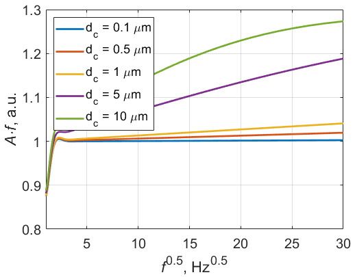
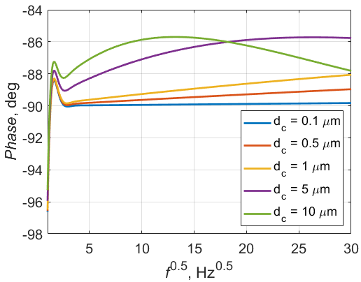
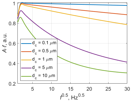
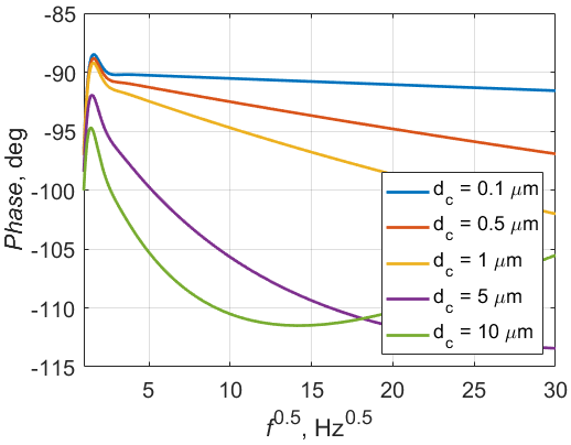
The theoretical amplitude and phase frequency characteristics presented in Fig. 1(a), 1(b), 1(c), and 1(d) were obtained for the thermal parameters of the example substrate of Cd1-xBexTe x = 1% crystal [22], with different thickness and different thermal parameters of the surface layer, computed in the frequency range from f = 1 Hz to 1 kHz.
Thermal diffusivity and conductivity of the thin layer were taken as a part of thermal diffusivity and conductivity of the substrate: λl = λs/wα, αl = αs/wα where: wα is the weighting factor. Factor wα was the same for thermal conductivity and thermal diffusivity. Literature data of the thermal parameters of the ground surface layers and bulk materials of several materials such as: Si, GaAs, GaN, and CdTe show that the thermal capacity of the ground surface layers and the bulk substrate ρc are the same. As a result, the weighting factor wα for the thermal conductivity and the thermal diffusivity is the same because α = λ/ρc. The following relationships take place:
\( \frac{e_l}{e_s}=\left(\frac{1}{w_\alpha}\right)^{0.5} ; \quad R_{l s}=\frac{\frac{e_l}{e_s}-1}{\frac{e_l}{e_s}+1} \) (5)
As a result, only two parameters must be extracted from the fitting of theoretical characteristics to experimental ones wα and d. They were determined in the two-parameter fitting procedure.
Values of the weighting parameter wα in the calcula-tions presented in Fig. 1 were taken to obtain different values of the thermal reflection coefficient Rls between the layer and the substrate. The value of Rls for the case (a), (b) was −0.11, while for the case (c), (d) it was 0.52. These calculations aimed to show the influence of the value of the thermal reflection coefficient Rls on a character of the amplitude and phase frequency characteristics.
Comparison of the figures (in Fig. 1) shows that the character of the theoretical characteristics, i.e., increasing or decreasing, depends mainly on the value of the thermal reflection coefficient of thermal waves between the layer and the substrate Rls.
For the measurements, a PA set-up with a microphone detection in the front configuration was applied. This method was extended to the case of a two-layer structure of the sample. The samples were illuminated with a modu-lated intensity beam of the laser light LuxX+515‑150 with a 515 nm wavelength corresponding to a photon energy 2.41 eV, bigger than the energy gap of the investigated samples. The PA signal was detected with a condenser microphone and measured with a lock-in amplifier (Stanford Research SR830). The measurements were computer-controlled and performed at room temperature. For calibration of the experimental set-up, a thermally thick, optically opaque glassy carbon reference sample exhibiting a perfect quality surface was used.
The experimental frequency amplitude and phase PA characteristics of a series of Cd1-xBexTe samples are presented below in Figs. 2–4. First measurements were performed from f = 1 Hz up to 1 kHz. However, for low frequencies of modulation, a much more complicated model had to be used because the substrate was thermally thin. For the measurements higher than 100 Hz, the substrate became thermally thick, and a much simpler thermal model could be applied. For this reason, the scope of measurements was limited to the frequencies higher than 100 Hz.
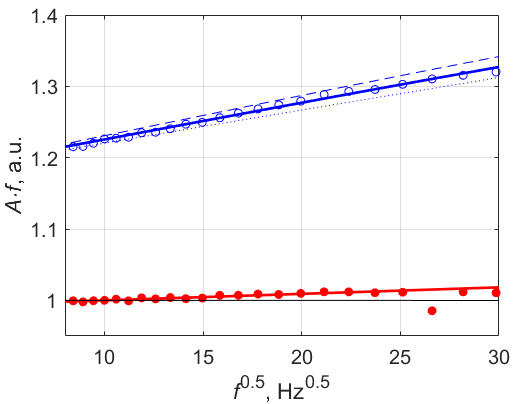
The experimental data and theoretical PA amplitude and phase characteristics obtained for the Cd1-xBexTe x = 1% sample are presented in Fig. 2. From the fitting procedure, the following weighting factors of the layer and the thermal reflection coefficient Rls were extracted: wα = 1.84, wλ = 1.84, d = 5.5 μm, Rls = −0.15.
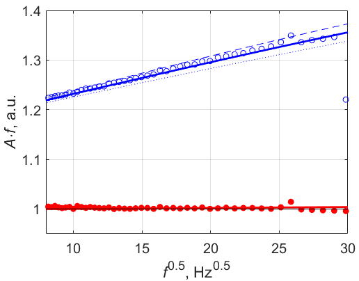
The experimental data and theoretical PA amplitude and phase characteristics obtained for the Cd1-xBexTe x = 3% sample are presented in Fig. 3. From the fitting procedure, the following weighting factors of the layer and the thermal reflection coefficient Rls were extracted: wα = 1.82, wλ = 1.82, d = 5.4 μm, Rls = −0.15.
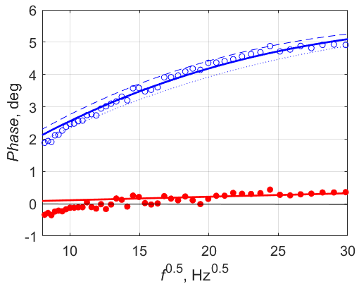
The experimental data and theoretical PA amplitude and phase characteristics obtained for the Cd1-xBexTe x = 10% sample are presented in Fig. 4. From the fitting procedure, the following weighting factors of the layer and the thermal reflection coefficient Rls were extracted: wα = 1.93, wλ = 1.93, d = 5.1 μm, Rls = −0.16. The collected values of the parameters extracted from the fitting procedure are presented in Table 2.
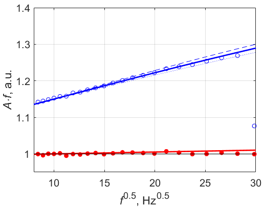
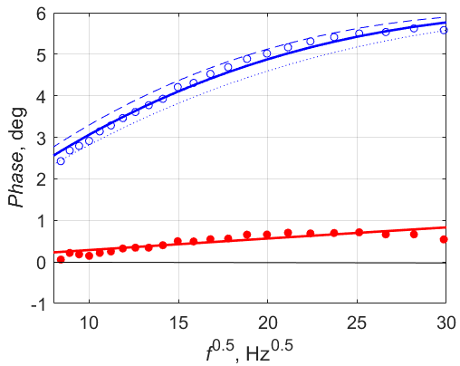
Table 2.
Physical parameters of the surface layers.
x% |
d [µm] |
wα |
es/el |
αl [cm2/s] |
λl [W/cmK] |
1 |
5.5 |
1.841 |
1.36 |
0.01955 |
0.023899 |
3 |
5.4 |
1.823 |
1.35 |
0.01157 |
0.013709 |
10 |
5.1 |
1.929 |
1.39 |
0.00824 |
0.010316 |
The first general conclusion that can be drawn from the amplitude characteristics of all ground samples is that the thermal effusivity of the surface layer must be smaller than that of the substrate. Only in this case, the amplitude of the PA signal of the ground sample is bigger than that of the substrate. What is more, the amplitude of the ground samples tends to about 1.30–1.35, respectively, to the polished samples at 900 Hz. It is close to es/el presented in Table 2. It is the case when the ground layers tend to become thermally thick.
Thanks to the procedure of a two-parameter fitting of theoretical characteristics to experimental PA amplitude and phase data, several surface layer parameters were extracted. Computer calculations in the two-parameter fitting procedure indicated that it was possible to extract two parameters of the surface layers simultaneously, i.e., the weighting parameter wα and the thickness of the surface layer d. As a result, thermal conductivity, thermal diffusivity, and thickness of the surface layers were determined. The following parameters of the surface layers were determined: thermal conductivity λl = λs/wα, thermal diffusivity αl = αs/wα, and thickness of the surface layer d. Among them, the thickness of the surface layer d was the most important as it carries information about the quality of the surface. Thermal conductivity and thermal diffusivity of the Cd1-xBexTe substrate taken for computa-tions are presented in [22]. In the experiment, the light penetration depth in the sample was smaller than about 0.1 μm, i.e., smaller than the thickness of the ground surface layer. It corresponded to the optical absorption coefficient of the sample, β = 105 cm−1, for the illuminating laser light.
For all investigated samples, the thickness of the surface layer after the grinding process was from about 5.1 μm to 5.5 μm. The thermal conductivity of the layers was about 1.8 times smaller, and the thermal diffusivity was also about 1.8 times smaller with respect to the thermal parameters of the substrate, i.e., the bulk material
The results of theoretical computations and experimental results presented in the paper show that it is possible to extract information about three parameters of a damaged layer in semiconductor samples with the PA method in the frequency domain. The research also showed the correctness of the proposed two-layer model of the PA signal in the front experimental configuration used to describe the PA signal of the thin surface layer on the thermally and optically thick substrate.
The experiments were performed on a series of Cd1‑xBexTe samples. They had differently prepared surfaces. The PA frequency characteristics were measured for the ground and polished samples. The ground samples showed the mechanically damaged surface layers of a thickness from about 5.1 μm to about 5.5 μm and thermal conductivities and diffusivities about 1.8 times worse than the substrate, i.e., the bulk material. The thickness of the mechanically damaged surface layers of the polished samples was less than 0.5 μm, making it impossible to determine their thermal parameters.
The advantage of the PA method in the front configuration is that it is a non-contact and non-destructive method. Thanks to the two-parameter fitting procedure of theoretical curves to experimental amplitude and phase PA characteristics, it was possible to simultaneously extract the thickness of the ground damaged layer, its thermal conductivity, and thermal diffusivity when only the thermal parameters of the substrate are known. The determination of the damaged layer thickness is based on the assumption that the heat capacity of the layer and the substrate is constant for each sample tested.
Research concept and design, L.B. and M.M.; collection of data, L.B. and Ł.Ch.; data analysis and interpretation, M.M, L.B., and Ł.Ch.; writing the article, M.M., Ł.Ch., and J.Z.; critical revision of the article, J.Z; final approval of article, M.M. and J.Z.; sample preparation, J.Z. and M.B.
Del Sordo, S. et al. Progress in the development of CdTe and CdZnTe semiconductor radiation detectors for astrophysical and medical applications. Sensors 9, 3491–3526 (2009). https://doi.org/10.3390/s90503491
Gnatyuk, V., Maslyanchuk, O., Solovan, M., Brus, V. & Aoki, T. CdTe X/γ-ray detectors with different contact materials. Sensors 21, 3518–3538 (2021). https://doi.org/10.3390/s21103518
Singh, D. et al. Innovative photovoltaic approach: Cd1-xBexTe mixed semiconductor crystal for novel dye-sensitized solar cells. Mater. Sci. Energy Technol. 7, 287–296 (2004). https://doi.org/10.1016/j.mset.2024.04.001
Lin, Q. et al. High-efficiency deep-red quantum-dot light-emitting diodes with type-II CdSe/CdTe core/shell quantum dots as emissive layers. J. Mater. Chem. C 49, 7223–7229 (2016). https://doi.org/10.1039/C6TC01531J
Chin, P. T. K., Stouwdam, J. W., van Bavel, S. S. & Janssen,R. A. J. Cluster synthesis of branched CdTe nanocrystals for use in light-emitting diodes. Nanotechnology 19, 205602 (2008). https://doi.org/10.1088/0957-4484/19/20/205602
Zakrzewski, J., Maliński, M., Boumhamdi, M., Strzelecki, J. & Strzałkowski, K. The new interpretation of the photothermal spectra of CdTe samples after different surface treatments. Crystals 14, 1019 (2024). https://doi.org/10.3390/cryst14121019
Zakrzewski, J., Maliński, M., Bachiri, A. & Strzałkowski, K. Photothermal determination of the optical and thermal parameters of CdxZn1-xSe mixed crystals. Mater. Sci. Eng. B 271, 115305 (2021). https://doi.org/10.1016/j.mseb.2021.115305
Zakrzewski, J., Strzałkowski, K., Maliński, M. & Chrobak, Ł. Two-layer model in piezoelectric photothermal spectra of CdTe crystals. Int. J. Thermophys. 40, 1–10 (2019). https://doi.org/10.1007/s10765-019-2521-5
Maliński, M. Application of the temperature distribution formula for the photoacoustic investigations of layer systems. Eur. Phys. J. Spec. Top. 153, 291–293 (2008). https://doi.org/10.1140/epjst/e2008-00448-x
Zakrzewski, J. et al. Photothermal determination of the surface treatment of Cd1-xBexTe mixed crystals. Appl. Sci. 13, 2113 (2023). https://doi.org/10.3390/app13042113
Chrobak, Ł. & Maliński, M. On investigations of the optical absorption coefficient of gold and germanium implanted silicon with the use of the non-destructive contactless photo thermal infrared radiometry. J. Electron. Mater. 48, 5273–5278 (2019). https://doi.org/10.1007/s11664-019-07333-0
Bychto, L., Maliński, M., Chrobak, Ł., Zakrzewski, J. & Boumhamdi, M. Investigations of optical and thermal properties of surface layers of Cd1-xBexTe samples by the photoacoustic method. Opto-Electron. Rev. 32, e150186 (2024). https://doi.org/10.24425/opelre.2024.150186
Maliński, M. & Chrobak, Ł. Numerical analysis of the photoacoustic spectra of silicon samples with differently treated surfaces. Opt. Commun. 283, 1004–1007 (2010). https://doi.org/10.1016/j.optcom.2009.11.029
Chrobak, Ł., Maliński, M., Zakrzewski, J. & Strzałkowski, K. The photoacoustic spectroscopic investigations of the surface preparation of ZnSe crystals. Surf. Sci. 603, 3282–3285 (2009). https://doi.org/10.1016/j.susc.2009.09.014
Maliński, M. & Chrobak, Ł. Numerical analysis of absorption and transmission spectra of silicon samples with differently treated surfaces. Opto-Electron. Rev. 19, 46–50 (2011). https://doi.org/10.2478/s11772-010-0064-1
Strzałkowski, K., Pawlak, M., Kulesza, S., Dadarlat, D. & Streza, M. Effect of the surface roughness on the measured thermal diffusivity of the ZnBeMnSe single crystalline solids. Appl. Phys. A 125, 459 (2019). https://doi.org/10.1007/s00339-019-2756-9
Todorović, D. M., Smiljanić, M., Sarajlić, M., Vasiljević-Redović, D. & Redjelović, D. Investigations of the effects of Ar plasma etching in Si surface by photoacoustic method. J. Phys. IV France 125, 451–453 (2005). https://doi.org/10.1051/jp4:2005125106
Todorović, D. M., Pawlak M., Delgadillo-Holtfort, I. & Pelzl, J. Photoacoustic and photothermal radiometry spectra of implanted Si wafers. Eur. Phys. J.: Spec. Top. 153, 259–262 (2008). https://doi.org/10.1140/epjst/e2008-00440-6
Todorović, D. M., Smiljanić, M., Jović, V., Sarajlić, M. & Grozdić, T. Investigation of interface and surface energy states in semiconductors by PA method. Eur. Phys. J.: Spec. Top. 153, 247– 250 (2008). https://doi.org/10.1140/epjst/e2008-00437-1
Al-Hamdi, T. K. et al. CdTe synthesis and crystal growth using the high-pressure Bridgman technique. J. Cryst. Growth 534, 125466 (2020). https://doi.org/10.1016/j.jcrysgro.2019.125466
Rudolph, P. & Mühlberg, M. Basic problems of vertical Bridgman growth of CdTe. Mater. Sci. Eng. B 16, 8–16 (1993). https://doi.org/10.1016/0921-5107(93)90005-8
Singh, D., Strzałkowski, K., Abouais, A. & Alaoui-Belghiti, A. Study of the thermal properties and lattice disorder effects in CdTe- based crystals: CdBeTe, CdMnTe, and CdZnTe. Crystals 12, 1555 (2022). https://doi.org/10.3390/cryst12111555