
Received 27 Jun. 2023
Received in revised form 09 Aug. 2023
Accepted 28 Aug. 2023
Available on-line 15 Oct. 2023
Keywords: Type I AlSb/GaSb superlattice; 8-band k·p perturbation theory; nextnano simulations; AlSb layer degradation.
This paper presents results of the characterisation of type I GaSb/AlSb superlattices (SLs) with a thin GaSb layer and varying thicknesses of an AlSb layer. Nextnano software was utilized to obtain spectral dependence of absorption and energy band structure. A superlattice (SL) with an energy bandgap of ~ 1.0 eV and reduced mismatch value was selected for experimental investigation. SLs with single (sample A) and double (sample B) AlSb barriers and a single AlSb layer (sample C) were fabricated using molecular beam epitaxy (MBE). Optical microscopy, high-resolution X-ray diffractometry, and photoluminescence were utilized for structural and optical characterisation. The presence of satellite and interference peaks in diffraction curves confirms the high crystal quality of superlattices. Photoluminescence signal associated with the superlattice was observed only for sample B and contained three low-intensity peaks: 1.03, 1.18, and 1.25 eV. The first peak was identified as the value of the energy bandgap of the SL. Other two peaks are related to optical transitions between defect states located at the interface between the SL and the top AlSb barrier. The time-dependent changes observed in the spectral characteristics are due to a modification of the SL/AlSb interface caused by the oxidation and hydroxylation of the AlSb layer.
Materials from a 6.1 Å semiconductor family such as AlSb, GaSb, InAs, and their heterostructures have been of great interest to electronic engineers for about 40 years [1–4]. Close lattice match of these materials (6.136 Å for AlSb, 6.095 Å for GaSb, 6.058 Å for InAs [2]) enables the production of high-quality heterostructures. In superlattices (SLs) created from these materials, interactions between the quantum-confined states across multiple layers are possible [5]. That is the main reason why these SLs are utilized to fabricate various devices, such as quantum cascade lasers (QCL) [6] and infrared photodetectors (PDs) [7–9]. In the latter, GaSb/AlSb SLs could play the role of an electron barrier in mid-wavelength infrared (MWIR) PDs [10]. GaSb/AlSb superlattice (SL) strained to GaSb can be successfully used as an electron barrier in junction instruments in which the p-type contact is located on top of the epitaxial structure, with the aforementioned SL just below it. In such a situation, the light-absorbing areas are not defective which does not deteriorate the performance of the instrument. The advantage of its use is the minimal band discontinuity occurring in the valence band which does not create parasitic potential barriers for holes.
Compared to InAs/GaSb and InAs/AlSb SLs [8, 11–14], GaSb/AlSb SLs are less often studied, especially SLs with a thin GaSb layer below 40–50 Å [15]. The cross-transition between T and X or L valleys results in a significant decrease of photoluminescence (PL) intensity in such SLs which in turn hinders their optical characterisation. To amplify the PL signal, the GaSb/AlSb SLs are usually placed between two AlSb barriers.
This paper focuses on the characterisation of a type I GaSb/AlSb SL with a thin GaSb layer below 40 Å and Eg of about 1.0 eV at 200 K. Based on theoretical calculations of energy bandgap for varying SL period thickness, the SL with reduced lattice mismatch, i.e., with reduced AlSb layer thickness, was chosen for further investigation. The AlSb layer was not too thin to hinder the growth of the heterostructure but thin enough to significantly reduce the SL lattice mismatch. The structural properties of SL and the calculated value of its bandgap energy were used to explain the optical properties of SL measured by the means of PL.
The experimental investigations were preceded and supported by theoretical calculations performed with the use of nextnano software-based 8-band k⋅p Kane’s model [16, 17]. In these calculations, energy eigenstates within quantum wells are obtained considering conduction, heavy- hole, and light-hole bands. As a result, the energy states in 11 ML GaSb/n ML AlSb SLs were calculated (n – number of AlSb monolayers in SL), as well as effective bandgap energy understood as a transition energy between first electron and heavy-hole state. Absorption spectra were also obtained from the calculations. The 11 ML GaSb/3 ML AlSb SL that meets the criteria of Eg ∼ 1.0 eV at elevated temperatures (T > 200 K) and a thin AlSb layer providing a low SL lattice mismatch (Δa) was chosen for experimental investigation.
Investigated samples were grown in the Riber 32P molecular beam epitaxy system. Source materials were evaporated from Knudsen (Al), SUMO (Ga), and valved cracker (Sb) cells. The cracker zone was constantly kept at 1000 °C. This provides the advantage of Sb1 particles over Sb2 in antimony molecular beam ensuring good optical quality of the material [18]. During the experiment, three samples were grown on (100) undoped (p-type) GaSb substrates: two (A and B) containing GaSb/AlSb SL, and one (C) consisting of a single AlSb layer. For each sample, first, a 300 nm GaSb buffer layer was applied and then it was followed by an AlSb (bottom) layer which was nominally 90 nm thick for sample A, 40 nm for sample B, and 70 nm for sample C. Then, in case of samples A and B, the 60-period GaSb/AlSb SL was grown. The nominal layer thickness of GaSb/AlSb SLs was 11 ML/3 ML. Sample B was additionally covered with AlSb top layer (see Fig. 1), so the bottom and top AlSb layers played the role of barriers for carriers localised in SL. Structures were not protected by any cover layer (e.g., GaSb) not to modify the structural and optical properties of SLs, for example by inducing strain.
The growth processes of all samples were performed under the same conditions. The temperature of the substrate during the growth of both GaSb buffer and AlSb barriers was 520 °C. GaSb/AlSb SLs were grown at a lowered substrate temperature of about 410 °C. The growth stopped while reaching the lower temperature. A growth temperature of 410 °C was selected through previous studies and, based on them, considered optimal. The temperatures were monitored using the RAYTEC Marathon pyrometer (spectral response peak at about 1640 nm). The V/III beam equivalent pressure ratio was 3.33 for GaSb and 2.13 for AlSb. The growth rates for AlSb and GaSb materials were 1.07 Å/s and 1.30 Å/s, respectively.
The optical quality of epi structures was evaluated using an optical microscope and PL spectroscopy. The images were taken with an OLYMPUS DSX510. The differential interference contrast module was used. The optical zoom of the lens was 10×, and the digital zoom was 4× Nicolet iS50R Fourier transform infrared (FTIR) spectrometer equipped with a quartz beam splitter and an MCT PD cooled with liquid nitrogen was used for PL measurements. During the measurement, the samples were placed in a Janis CCS-150 cryostat and illuminated with a 808 nm laser line with a laser spot of 10-4 cm2 and a laser power varying from 0.7 mW to 72 mW, yielding the excitation power density range from 7 W/cm2 to 720 W/cm2. The spectra were collected in a temperature range from 14 K to 150 K (however, for temperatures higher than 100 K, the output signal faded). Structural characterisation was performed with the use of a high-resolution X-ray diffractometry (HRXRD). The used diffractometer was a PANalytical X’Pert PRO. Specification details of the HRXRD station are included in Ref. 19.
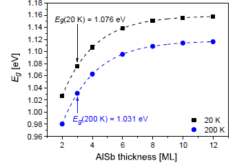
Before experimental investigations, the band structure and the absorption coefficient were calculated using nextnano software. The aim was to find the SL with an effective energy bandgap Eg ∼ 1.0 eV at 200 K and employ reduced AlSb layer thickness. The temperature of 200 K was chosen because it is achievable by a thermoelectrical cooler utilized in high-operating-temperature (HOT) photodetectors [20]. The theoretical calculations yielded the energies of the first electron (E1), heavy-hole (HH), and light-hole (LH) states. Eg was defined as E1-HH transition energy of which values at 20 K and 200 K for SLs with 11 ML GaSb layer and varying AlSb thickness are presented in Fig. 2. As it can be seen, Eg of around 1.03 eV at 200 K was obtained for the 11 ML GaSb/3 ML AlSb SL and, therefore, it was chosen for further experimental investigations. The strain has been taken into account during calculations. The dashed lines are representing exponential fit to calculated values.
The spectral dependence of the calculated absorption coefficient at 20 K is shown in Fig. 3. E1-HH and E1-LH transition energies are marked by the arrows in the figure. The transition energy between E1 and HH determines Eg = 1.076 eV which corresponds to a cut-off wavelength of λc = 1.151 μm. Transition energy between E1 and LH is equal to 1.103 eV (λc = 1.123 μm). The absorption spectrum was obtained by the self-consistent solution of the system of Schrödinger and Poisson equations using the 8-band k⋅p method. As a result, an electronic band structure was calcu- lated around the Gamma point within a cuboid reaching 10% of the distance from the Gamma point to the borders of the First Brillouin Zone on the 16 × 16 × 16 wavevector grid. Also, the Fermi level was obtained during the process. Results were further interpolated to a 5 times finer grid of wavevectors and passed to a standard absorption model based on Fermi’s Golden Rule with the polarisation of the optical field assumed to be perpendicular to the growth direction polarisation TE. A broadening of 10 meV was assumed.
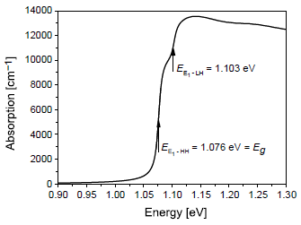
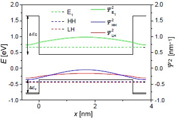
Fig. 4 shows the band structure of 11 ML GaSb/ 3 ML AlSb SL at 20 K. The black solid lines represent E1, LH, and HH states for bulk materials. The probability densities of carriers Ψ² and offset values (ΔEc = 1.215 eV, ΔEv = 0.406 eV) are also shown in Fig. 4. It can be noted that the probability density of carriers for the HH state is higher than for the LH state which is due to lower transition energy. Moreover, the lower probability density of carriers for LH is due to the spreading of the wavefunction in the AlSb layer due to its effective masses and its confinement in the GaSb quantum well.
The accuracy of the performed calculations is about 20 meV. It was estimated in two steps. Firstly, the correctness of parameters chosen for calculations has been confirmed by performing calculations for superlattices at 16 K described in Ref. 21. An agreement for fundamental transition energy better than ∼ 10 meV has been observed.
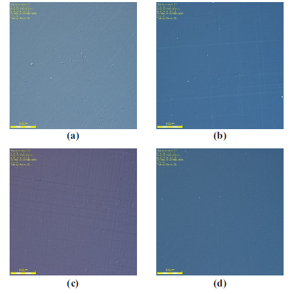
Secondly, based on results obtained for type II SL [22, 23], interface effects (not included here) have been estimated to be in the order of magnitude of ∼ 10 meV [22]. Fig. 5 shows microscope images of the surface of investigated samples taken on the day of growth and for sample B taken five weeks later. In general, the surfaces of all investigated samples were similar as the thickness of relaxed AlSb materials was in the range of 70 nm–90 nm. The cross-hatch pattern of dislocations and the few round- shaped defects reaching up to 10 μm in diameter are visible.
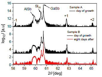
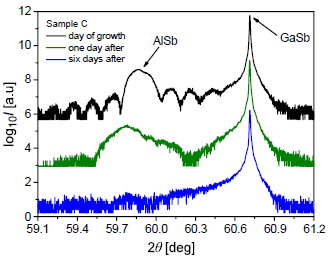
The XRD measurements consisting of 2θ/ω curves allowed for the determination of SL period thickness, thick- nesses of component layers, and values of perpendicular lattice mismatch (Δa/a)⊥ of GaSb/AlSb SLs and AlSb layer. The 2θ/ω curves for samples A and B are presented in Fig. 6, while Fig. 7 shows the results for the AlSb single layer (sample C). Both figures contain 2θ/ω curves measured several days apart.
The analysis of 2θ/ω curves allowed for determination of the thicknesses of the GaSb and AlSb layers in SLs and the perpendicular lattice mismatch (Δa/a)⊥ to GaSb buffer for SLs (samples A and B) and AlSb layer (sample C). The (Δa/a)⊥ to the buffer for SLs or AlSb is defined as in Ref. 24 and described as follows:
\( \left(\frac{\Delta a}{a}\right)_{\perp}=\frac{a_{\perp_{\mathrm{SL}_0 / \mathrm{Also}}}-a_{\perp_{\mathrm{GaSb}}}}{a_{\perp_{\mathrm{GaSb}}}} \) (1)
where a⊥SL /AlSb is the perpendicular lattice constant of the GaSb/AlSb SL (or AlSb) for which lattice mismatch is calculated, and a⊥GaSb is the perpendicular lattice constant for GaSb buffer. All calculated values are shown in Table 1. It can be noticed that obtained SLs were a bit thicker than expected.
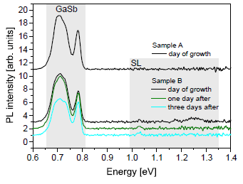
PL measurements were employed to investigate the optical quality of samples. The spectra were collected for samples A and B, however, the PL signal associated with SL was detected only for sample B, see Fig. 8. It can be noted that all spectra exhibit a wide band located in the range of 0.65 eV–0.83 eV, containing several peaks originating from GaSb material, the most distinguishable ones being 0.686 eV (phonon replica of 0.708 eV line), 0.708 eV (acceptor), 0.728 eV (phonon replica of 0.757 eV line), 0.757 eV (acceptor), and 0.783 eV (native acceptor) [25, 26]. For sample B, the spectra were measured several times. It can be seen that the PL spectrum measured on the first day (black curve) contains three peaks of low intensity placed at about 1.03 eV, 1.18 eV, and 1.25 eV, while the spectra measured on one day and three days after growth (green and cyan curves, respectively) contain only peak at 1.03 eV. The PL spectrum of sample A does not exhibit any peaks in this range. The lack of PL signal from the SL of sample A is probably due to the escape of carriers from the SL material and their non-radiative recombination on surface states.
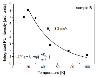
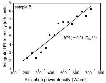
Due to the low intensity and asymmetry of the 1.03 eV peak, it was difficult to establish the thermal dependence of the PL peak energy. However, it was possible to determine the relationship between the integrated PL intensity and temperature, as well as excitation power density. The thermal characteristic was fitted by the one-channel non- radiative recombination model [27] and the activation energy was calculated in the low-temperature region (see Fig. 9). The linear characteristic of the integrated PL intensity on the excitation power for a 1.03 eV peak was also obtained and presented in Fig. 10. It was fitted using relation I(PL) ∼ E k [28], while k parameter was determined to be close to unity.
The simulations allowed for the determination of the effective energy bandgap for 11 ML GaSb/n ML AlSb SLs (n ML – number of AlSb monolayers). They indicated that 11 ML GaSb/3 ML AlSb SL meets the criteria of Eg ∼ 1.0 eV and that the reduced thin AlSb layer in each period results in a decreased SL lattice mismatch (2700 ppm). The absorption spectra calculated for T = 20 K revealed two optical transitions: one at 1.076 eV, between E1 and HH which is equivalent to effective bandgap Eg, and at 1.103 eV which is related to the transition between E1 and LH. The probability density of carriers for HH states being higher than for LH states suggests that a PL peak at 1.076 eV is expected to appear in the PL spectrum for the chosen SL.
To prevent carriers from escaping from the SL region into the GaSb buffer, an AlSb layer was used as a potential barrier. The thickness of the AlSb barrier was higher than the critical value for this material (which is 41 nm, according to Matthews-Blakeslee theory [29]), above which the lattice stress relaxation begins. It is demonstrated in Fig. 5(a), 5(b), and 5(c) by a dislocation cross-hatch seen for all investigated samples. It is worth noting that the lowest density of dislocation lines occurs for sample A due to the filtering role of the SL [30]. For sample B, the visible dislocations originate mainly from the relaxed 40 nm AlSb top barrier deposited on strained SL. The densest cross- hatch is observed for sample C. In this case, the dislocations are generated at the interface between the thick 70 nm AlSb layer and GaSb buffer.
There is no SL filter, all dislocations originating from the misfit relaxation propagate through the AlSb layer and reach the surface. The interesting feature is visible in Fig. 5(d) which shows the surface image of sample B taken five weeks after it was grown. Comparing the two images of sample B presented in Fig. 5(b) and 5(d), it can be seen that the initially visible cross-hatch almost disappeared. The same was observed for sample C (AlSb single layer, not shown) while the surface of sample A (with buried AlSb buffer) has not changed because of termination by the GaSb layer. The common factor in the investigated samples B and C is the AlSb layer with a free surface that degraded due to oxidation. The HRXRD measurements provided further information proving this statement. 2θ/ω profiles of samples A and B (Fig. 6) were very similar, except for AlSb related peak. Superlattice peaks of the −1st and +2nd order were observed on HRXRD curves. Intense and narrow satellites prove the constant period thickness during the growth process and high crystal quality of investigated SLs. The full width at half maximum (FWHM) of AlSb material peaks for samples A, B, and C are 0.104 deg, 0.209 deg, and 0.137 deg, respectively. It means that FWHM values for samples A and C are similar and almost twice smaller than for sample B.
It results from differences in lattice constants of AlSb layers modified by the lattice constant of underneath material in analysed samples. The lattice constants of AlSb layers in samples A and C are similar because AlSb material was deposited on GaSb material. In the case of sample B, the lower AlSb layer was deposited on the GaSb material and the upper one on the SL material, hence the differences in the lattice constants. As a result, there are two partially overlapping peaks in the 2θ/ω curves with a wider FWHM than for the single peak. The curves for sample B measured immediately after the growth process (black line in Fig. 6) and eight days later (red line) show a difference only for the AlSb peak while SL0 and satellite peaks remain the same. In the black 2θ/ω curve, one peak in the angular position of AlSb is observed while in the red curve measured eight days later the split peak shifted in the direction of lower angles is visible. A similar situation was observed for a single AlSb layer (sample C). In Fig. 7, three curves measured several days apart show the disappearance of the HRXRD signal from the AlSb layer. Moreover, the shift of the AlSb peak in the direction of lower angles is also clearly visible. This is most probably caused by the diffusion of oxygen atoms into the AlSb layer and its oxidation. Such an interpretation would be consistent with the conclusions drawn in Ref. 31. The authors claim that AlSb is prone to oxidation or hydroxylation simply by air exposure. They show that during air exposure, the 150 Å fully oxidized amorphous layer is formed first. Then H2O molecules from the air diffuse through the oxide to the transitional, partly oxidized region, resulting in the creation of aluminium hydroxide. This mechanism occurs according to the chemical reaction:
\( \mathrm{AlSb}+3 \mathrm{H}_2 \mathrm{O} \rightarrow \mathrm{Al}(\mathrm{OH})_3+\mathrm{SbH}_3 \) (2)
The aluminium hydroxide is therefore responsible for AlSb deterioration rather than aluminium oxide. Thus, the degradation of the AlSb top layer can justify the broadening of the AlSb layer peak in the 2θ/ω profile measured for sample B as compared to sample A in which the AlSb layer was buried in the structure. In standard temperature and pressure, SbH3 is a gas, however, it does not evaporate from the sample surface (in contrast to AlAs, where AsH3 does [31]). It is probably because stable oxidation and hydration products are obtained according to the reactions:
\( 2 \mathrm{SbH}_3+3 \mathrm{H}_2 \mathrm{O} \rightarrow \mathrm{Sb}_2 \mathrm{O}_3+6 \mathrm{H}_2 \) (3)
\( 2 \mathrm{SbH}_3+4 \mathrm{H}_2 \mathrm{O} \rightarrow \mathrm{Sb}_2 \mathrm{O}_4+7 \mathrm{H}_2 \) (4)
\( 2 \mathrm{SbH}_3+5 \mathrm{H}_2 \mathrm{O} \rightarrow \mathrm{Sb}_2 \mathrm{O}_5+8 \mathrm{H}_2 \) (5)
These hygroscopic properties of AlSb can be also responsible for disappearance of PL peaks from sample B. Three peaks of low intensity located at about 1.03 eV, 1.18 eV, and 1.24 eV were observed in the PL spectrum measured on the day of growth (see the black line for sample B in Fig. 8). First peak at 1.03 eV is relatively close to the theoretically estimated E1-HH transition of about 1.076 eV at T = 20 K for 11 ML GaSb/3 ML AlSb SL (Fig. 2). Taking into account the accuracy of calculations of ∼ 20 meV and thicker GaSb layer of 11.5 ML deter- mined from analysis of 2θ/ω curve (sample B) instead of 11.0 ML assumed for calculations, the energy of E1-HH transition should be 1.043 eV. This value differs only by 13 meV from the measured one of 1.03 eV. The second peak of 1.180 eV differs significantly from the calculated value for the E1-LH transition of 1.103 eV (Fig. 3) even when the calculation accuracy of ∼ 20 meV is taken into account. The peak at 1.24 eV is unidentified. It indicates that the optical transitions observed in PL are different from those obtained from simulations, except for the E1-HH transition. PL spectra collected on one day and three days after growth (green and cyan curves, respectively) show different pictures – peaks at 1.18 eV and 1.25 eV dis- appeared, whereas the peak at 1.03 eV interpreted by the authors as E1-HH transition remained almost unchanged. Higher energy PL peaks can be associated with the optical transitions between defect states located at SL/AlSb top barrier interface. The lack of these peaks in the spectrum of sample A seems to prove this statement. Hydroxylation of AlSb could modify the chemical composition of the interface, as well as defect states which may have led to the disappearance of these peaks.
The fitting of the thermal characteristic of the integrated PL intensity allowed to obtain an activation energy of 8.2 meV for the non- radiative process in a low-temperature region (Fig. 9). The optical quality of investigated SL (sample B) is proven by a linear characteristic of the integrated PL intensity as a function of the excitation power density. This dependence was fitted using exponential relation I(PL) ∼ Eexc k Obtained value of the k parameter equal to 1.05 indicates excitonic domination of the recombination process. It means that the optical quality of SL material is very high, including the geometrical and chemical abruptness of interfaces. It is worth noting that the lack of PL signal from SL of sample A is probably due to the escape of carriers from the SL material and their non-radiative recombination on surface states.
The two samples of GaSb/AlSb SLs and one consisting of a single AlSb layer were performed using the MBE technique. Structural characterisation of the heterostructures was carried out with the use of HRXRD while optical quality and properties were investigated with the use of a microscope and PL. The high structural quality of SLs has been proved by the presence of satellite peaks in 2θ/ω curves. Samples A and B differed only in the peaks related to the AlSb layer. The AlSb peak of sample B was asymmetric and broadened and changed with time. The peak related to AlSb single layer (sample C) disappeared six days after the sample was grown. The cross-hatch of dislocation lines was observed for all samples on the day of growth and they almost disappeared after a few days. The common reason for these changes is the hygroscopic property of AlSb which results in the formation of aluminium hydroxide and material degradation. The PL signal associated with SL was detected only for sample B with bottom and top AlSb barriers. Three peaks were measured in the PL spectrum: at 1.03 eV, 1.18 eV, and 1.24 eV. Two higher energy peaks disappeared after a few days from the day of growth, while the peak at 1.03 eV remained unchanged. PL peak at 1.03 eV is associated with the transition between the first electron (E1) and heavy-hole (HH) states. The energy of E1-HH transition calculated using nextnano software for 11.5 ML GaSb/3ML AlSb SL is 1.043 eV, if the calculation accuracy of ∼ 20 meV is taken into account which stays in good agreement with the experimentally obtained value of 1.030 eV. The activation energy of 8.2 meV for the non-radiative process in a low- temperature region of 14 K–100 K was determined from the thermal dependence of the integrated PL intensity. The optical quality of the investigated SL has been proved by a linear characteristic of the integrated PL intensity vs. the excitation power density. This dependence was fitted using the exponential relation with a k parameter equal to 1.05. It indicates that the dominant recombination process is mainly radiative and exciton-dominated. GaSb/AlSb SLs with an effective bandgap of 1.03 eV at 20 K (about 1.0 eV at 200 K) and a reduced lattice mismatch of 2700 ppm can be used as barriers in MWIR photodetectors working in HOT conditions.
The research was carried out as part of the “Implementation Doctorate” program of the Ministry of Education and Science in Poland, project no. DWD/6/0216/2022, and partially funded by the National Center for Research and Development (NCBR) from the project TECHMATSTRATEG-III/0038/2019-00.
Aspnes, D. E. & Studna, A. A. Dielectric functions and optical parameters of Si, Ge, GaP, GaAs, GaSb, InP, InAs, and InSb from 1.5 to 6.0 eV. Phys. Rev. B 27, 985–1009 (1983). https://doi.org/10.1103/PhysRevB.27.985
Chang, C. A., Takaoka, H., Chang, L. L. & Esaki, L. Molecular beam epitaxy of AlSb. Appl. Phys. Lett. 40, 983–985 (1982). https://doi.org/10.1063/1.92976
Takaoka, H., Chang, C.-A., Mendez, E. E., Chang, L. L. & Esaki, L. GaSb/AlSb/InAs multi-heterojunctions.Physica B+C 117, 741–743 (1983). https://doi.org/10.1016/0378-4363(83)90639-3
Mendez, E. E., Chang, C.-A., Takaoka, H., Chang, L. L. & Esaki, L. Optical properties of GaSb–AlSb superlattices. J. Vac. Sci.Technol. B 1, 152–154 (1983). https://doi.org/10.1116/1.582521
Alam, M. N., Matson, J. R., Sohr, P., Caldwell, J. D. & Law, S. Interface quality in GaSb/AlSb short period superlattices. J. Vac. Sci.Technol. A 39, 063406 (2021). https://doi.org/10.1116/6.0001290
Baranov, A. N. & Teissier, R. Quantum cascade lasers in the InAs/AlSb material system. IEEE J. Sel. Top. Quantum Electron. 21, 85–96 (2015). https://doi.org/10.1109/JSTQE.2015.2426412
Ting, D. Z. et al. InAs/InAsSb superlattice infrared detectors. Opto- Electron. Rev. 31, e144565 (2023). https://doi.org/10.24425/opelre.2023.144565
Rodriguez, J. B., Christol, P., Cerutti, L., Chevrier, F. & Joullié, A. MBE growth and characterization of type-II InAs/GaSb superlattices for mid-infrared detection. J. Cryst. Growth 274, 6–13 (2005). https://doi.org/10.1016/j.jcrysgro.2004.09.088
Müller, R. et al. Thermoelectrically-cooled InAs/GaSb type-II superlattice detectors as an alternative to HgCdTe in a real-time mid- infrared backscattering spectroscopy system. Micromachines (Basel) 11, 1124 (2020). https://doi.org/10.3390/mi11121124
Gautam, N. et al. Band engineered HOT midwave infrared detectors based on type-II InAs/GaSb strained layer superlattices. Infrared Phys. Technol. 59, 72–77 (2013). https://doi.org/10.1016/j.infrared.2012.12.017
Delmas, M., Liang, B. L. & Huffaker, D. L. A comprehensive set of simulation tools to model and design high-performance Type-II InAs/GaSb superlattice infrared detectors. Proc. SPIE 10926, 29–39 (2019). https://doi.org/10.1117/12.2509480
Spitzer, J. et al. Influence of the interface composition of InAs/AlSb superlattices on their optical and structural properties. J. Appl. Phys. 77, 811–820 (1995). https://doi.org/10.1063/1.359004
Rygała, M. et al. Investigating the physics of higher-order optical transitions in InAs/GaSb superlattices. Phys. Rev. B 104, 085410 (2021). https://doi.org/10.1103/PhysRevB.104.085410
Wróbel, J. et al. Investigation of a near mid-gap trap energy level in mid-wavelength infrared InAs/GaSb type-II superlattices. Semicond. Sci. Technol. 30, 115004 (2015). https://doi.org/10.1088/0268-1242/30/11/115004
Griffiths, G., Mohammed, K., Subbana, S., Kroemer, H. & Merz, J. L. GaSb/AlSb multiquantum well structures: Molecular beam epitaxial growth and narrow‐well photoluminescence. Appl. Phys. Lett. 43, 1059–1061 (1983). https://doi.org/10.1063/1.94235
Birner, S. et al. nextnano: General Purpose 3-D Simulations. IEEE Trans. Electron. Devices 54, 2137–2142 (2007). https://doi.org/10.1109/TED.2007.902871
Trellakis, A. et al. The 3D nanometer device project nextnano: Concepts, methods, results. J. Comput. Electron. 5, 285–289 (2006). https://doi.org/10.1007/s10825-006-0005-x
Xie, Q., Van Nostrand, J E., Jones, R. L., Sizelove, J. & Look, D. C. Electrical and optical properties of undoped GaSb grown by molecular beam epitaxy using cracked Sb1 and Sb2. J. Cryst. Growth 207, 255–265 (1999). https://doi.org/10.1016/S0022-0248(99)00379-6
Sankowska, I. et al. On the onset of strain relaxation in the Al0. 45Ga0. 55As/In Ga1− As active region in quantum cascade laser structures. J. Appl. Crystallogr. 50, 1376–1381 (2017). https://doi.org/10.1107/S1600576717011815
Martyniuk, P. & Rogalski, A. HOT infrared photodetectors. Opto- Electron. Rev. 21, 239–257 (2013). https://doi.org/10.2478/s11772-013-0090-x
Toyota, H. et al. Growth and characterization of GaSb/AlSb multiple quantum well structures on Si (111) and Si (001) substrates. Phys. Procedia 3, 1345–1350 (2010). https://doi.org/10.1016/j.phpro.2010.01.189
Delmas, M., Liang, B. L. & Huffaker, D. L. A comprehensive set of simulation tools to model and design high-performance Type-II InAs/GaSb superlattice infrared detectors. Proc. SPIE 10926, 29–39 (2019). https://doi.org/10.1117/12.2509480
Livneh, Y. et al. k·p model for the energy dispersions and absorption spectra of InAs/GaSb type-II superlattices. Phys. Rev. B 86, 235311 (2012). https://doi.org/10.1103/PhysRevB.86.235311
Czuba, K., Ciura, Ł., Sankowska, I., Papis-Polakowska, E. & Jasik, A. The role of noise in specific detectivity of InAs/GaSb superlattice MWIR bariodes. Sensors 21, 7005 (2021). https://doi.org/10.3390/s21217005
Jakowetz, W., Rühle, W., Breuninger, K. & Pilkuhn, M. Lumine- scence and photoconductivity of undoped p‐GaSb. Phys. Status Solidi A, 12, 169–174 (1972). https://doi.org/10.1515/9783112480687-018
Lee, M., Nicholas, D. J., Singer, K. E. & Hamilton, B. A. Photoluminescence and Hall‐effect study of GaSb grown by molecular‐beam epitaxy. J. Appl. Phys. 59, 2895–2900 (1986). https://doi.org/10.1063/1.336948
Lambkin, J. D. et al. Temperature dependence of the photolumines- cence intensity of ordered and disordered In0. 48Ga0. 52P. Appl.Phys. Lett. 65, 73–75 (1994). https://doi.org/10.1063/1.113078
Seetoh, I. P., Soh, C. B., Fitzgerald, E. A. & Chua, S. J. Auger recombination as the dominant recombination process in indium nitride at low temperatures during steady-state photoluminescence. Appl. Phys. Lett. 102, 101112 (2013). https://doi.org/10.1063/1.4795793
Matthews, J. W. & Blakeslee, A. E. Defects in epitaxial multilayers: I. Misfit dislocations. J. Cryst. Growth 27, 118–125 (1974). https://doi.org/10.1016/S0022-0248(74)80055-2
Hao, R. et al. Molecular beam epitaxy of GaSb on GaAs substrates with AlSb/GaSb compound buffer layers. Thin Solid Films 519, 228–230 (2010). https://doi.org/10.1016/j.tsf.2010.08.001
Nakata, J., Shibata, T., Nanishi, Y. & Fujimoto, M. Suppression of AlSb oxidation with hydrocarbon passivation layer induced by MeV‐He+ irradiation. J. Appl. Phys. 76, 2078–2085 (1994). https://doi.org/10.1063/1.357617