New generation of uncooled thermal detectors: A review
Antoni Rogalski*
Article Info
Received 17 Dec. 2025
Received in revised form 23 Mar. 2026
Accepted 30 Mar. 2026
Available on-line 30 Apr. 2026
Keywords: thermal detectors; low-dimensional solids; thermopiles; bolometers; pyroelectric detectors; photothermoelectric effect. resonator, and CMOS-compatible detectors.
Abstract
At the current stage of development of infrared detector technology in the long-wave infrared range, the only detector arrays available on the market that operate at room temperature are thermal detectors. Among these, monolithic microbolometer arrays are the most popular with production volumes exceeding those of all other infrared array technologies combined. However, the efficiency of thermal detectors is modest; they exhibit a slow response time and are not very useful for multispectral detection. For this reason, new ideas for thermal detector designs and new materials that meet the expected performance requirements are being sought. High hopes are pinned on a new generation of thermal detectors based on low- dimensional solid (LDS) materials. It is predicted that the fundamental properties of LDS thermal detectors, driven by the quantum-size effect, enable them to overcome the performance limitations of conventional bulk detectors. This paper aims to organise existing knowledge on this subject, compile current detector performance data, and identify potential directions for further development. It focuses on several types of thermal detectors operating at room temperature: photothermoelectric, bolometric, pyroelectric, nanoelectromechanical resonator, and CMOS-compatible detectors.
1. Introduction
Over the past 20 years, significant progress in nanofabrication has led to the development of a new generation of photodetectors. Within this broad class of detectors, photon detectors fabricated from low-dimensional solid (LDS) materials are of paramount importance. Among the latter, we can distinguish two-dimensional (2D) materials, nanowires/quantum dots, perovskites, and organic materials. They operate over a wide wavelength range, spanning from ultraviolet to far-infrared (IR).
The fundamental properties of LDS thermal detectors, determined by the quantum-size effect, enable them to circumvent the performance limitations of conventional bulk detectors. So far, however, the new generation of thermal sensors has been less popular than their counterparts that use photonic phenomena.
The paper first explains the basic principles of thermal sensors. Then, the latest developments in LDS thermal sensors were reviewed in the following order: thermoelectric, pyroelectric, bolometric, and nanoelectromechanical resonator detectors. More attention was given to the latter. In the final part of the paper, the performance of the new generation of thermal sensors was compared with that of detectors dominating the commercial market. Finally, the paper examines the primary challenges confronting LDS thermal detectors and provides projections for their future development prospects.
2. Principle of thermal detectors operation
Optical detectors are divided into two broad categories: photon detectors (also known as quantum detectors) and thermal detectors [1–6]. In the thermal detector, schematically shown in Fig. 1, incident radiation is absorbed, causing a change in the material temperature and the resulting change in a physical property is used to generate an electrical signal. The detector is suspended on legs (with high thermal resistance to isolate it from the surroundings as much as possible) connected to a heat sink. The signal is independent of the photonic nature of the incident radiation. Spectral sensitivity can be broad when the incident radiation is absorbed by the black coating covering the detector.
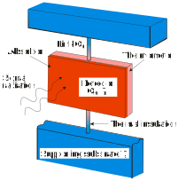
Fig. 1. Schematic diagram of a thermal detector.
Figure 2 shows the relative response of detectors as a function of wavelength, with the vertical scale W-1 or photon-1. In general, thermal detectors exhibit a flat spectral response (their sensitivity is proportional to the absorbed energy), whereas photonic detectors have a constant spectral sensitivity per photon [see Fig. 2(b)]. For thermal detectors, the signal depends on the radiation power (or its rate of change), but not on its spectral content.
Photon detectors are characterised by their selective sensitivity, which depends on wavelength per unit of incident radiation power. Their response is proportional to the incident photon frequency (photon energy is inversely proportional to wavelength). Thus, the spectral responsivity increases linearly with wavelength [see Fig. 2(a)] until it reaches a long-wavelength sensitivity limit, determined by the energy gap of the detector material. The cut-off wavelength is typically defined as the point at which the detector sensitivity drops to 50% of its maximum value.
Among thermal detectors, the most widely used are bolometers, pyroelectric detectors, and thermoelectric detectors. The thermopile is one of the oldest IR detectors, consisting of a series-connected thermocouple array to achieve improved temperature sensitivity. In pyroelectric detectors, the signal is generated by a change in internal electrical polarisation in response to incident radiation, whereas in thermistor bolometers, it is generated by a change in electrical resistance. For a long time, thermopiles were considered slow, insensitive, bulky, and expensive devices. However, thanks to advances in semiconductor technology (micromechanics, photolithography, selective etching, etc.), thermopile performance has been optimised for specific applications. Over the last few decades, thanks to conventional complementary metal-oxide semiconductor (CMOS) processes, thermopile integrated circuit technology has enabled mass production.
Typically, a bolometer is a thin, blackened element/slab whose impedance strongly depends on temperature. Bolometers can be divided into several types. The most commonly used types are metal bolometers, thermistor bolometers, and semiconductor bolometers. The fourth type is the superconducting bolometer. The latter operates based on a conduction transition, in which the resistance changes drastically over the transition temperature range. Figure 3 schematically illustrates the temperature dependence of resistance for four different types of bolometers.
Currently, IR microbolometer detectors are produced in larger volumes than all other IR array technologies combined. Among them, vanadium oxide (VOx) microbolometer arrays are by far the most widely used uncooled detector technology. VOx wins the competition between amorphous silicon bolometers and ferroelectric barium strontium titanate (BST) detectors. The principle of vanadium dioxide (VO2) operation is a phase transition
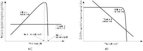
Fig. 2. Relative
spectral response for a photon and thermal detectors: (a) at constant incident radiant power, (b) at
constant photon flux.
Relative spectral response per Watt Relative spectral response per photon
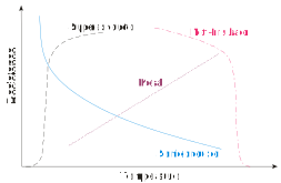
Fig. 3. Temperature dependence of resistance of three bolometer material types.
from a low-temperature insulating phase to a hightemperature metallic phase, as shown in Fig. 3. This phase transition is explained by the Mott insulator model.
Various types of thermal detectors operate across a wide spectral range of electromagnetic radiation. Their operating principles are briefly described in Table 1.
Thermal detectors.
| Mode of operation | Schematic of the detector | Operation and properties |
|---|---|---|
| Thermopile |
|
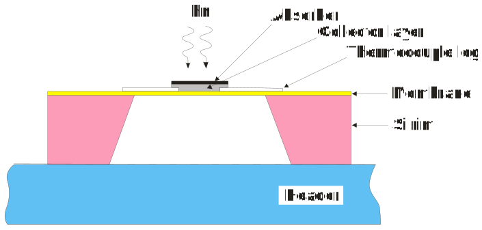
A thermocouple is typically a thin, blackened flake thermally bonded to the junction of two dissimilar metals or semiconductors. The increase in junction temperature due to radiation absorption generates a signal proportional to the thermoelectric electromotive force. Although thermocouples are not as sensitive as bolometers and pyroelectric detectors, they are widely used for their reliability and good cost-to-performance ratio. A particular area of application is spectroscopy. |
| Photothermoelectric detector |
|
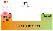
The photothermoelectric (PTE) effect is a derivative of the thermoelectric (TE) effect and is caused by uneven illumination. It can also be caused by significant differences in absorption across different parts of the detector active area. For example, the figure on the left shows the effect of light-induced heating in a semiconductor channel (e.g., in a field-effect transistor), which creates a temperature gradient. |
|
Bolometer Metal Semiconductor Superconductor Hot electrons |
|
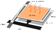
A bolometer is a resistive element made of a material with a very low thermal capacity and a high-temperature coefficient. When these conditions are met, absorbed radiation causes a large change in resistance. This resistance change is similar to that of a photoconductor, but their detection mechanisms are different. In a bolometer, the incident radiation generates heat in the material, which in turn changes the resistance. Instead of a direct photon-electron interaction, as in photon detectors, the interaction is electron-phonon. Initially, most bolometers were made of manganese, cobalt, or nickel oxides. Currently, microbolometers (whose active areas consist mainly of vanadium oxide or amorphous silicon) are manufactured in large-format matrices for thermal imaging. Some extremely sensitive semiconductor and superconducting bolometers operating at low temperatures are used in the THz range. |
| Pyroelectric detector |
|
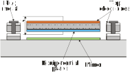
A pyroelectric detector is essentially a small capacitor with two conductive electrodes mounted perpendicular to the direction of a spontaneous polarisation of the capacitor material. Incident radiation changes the polarisation, resulting in the appearance of a charge on a capacitor and the current generation. The value of this current depends on the temperature increase and the material pyroelectric coefficient. To generate a current, the incoming signal must be interrupted or modulated. Usually, the detector sensitivity is limited by amplifier noise or tangential noise. The detector response speed can be adjusted over a wide range. Thanks to this, pyroelectric detectors are also used to detect fast laser pulses, but at the cost of reduced sensitivity. |
| Golay cell |
|
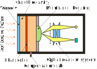
A Golay cell is a hermetically sealed container filled with gas (usually xenon due to its low thermal conductivity). It is designed so that the expansion of gas due to the incident radiation heat deforms a flexible membrane. The membrane deflection is monitored by an optical system, a capacitive detector, or a tunneling displacement transducer. To increase the gas absorption of IR radiation, the chamber is equipped with an additional absorber. Another way to increase absorption is to use reflective walls in a cavity. The performance of the Golay cell is limited only by thermal noise arising from heat transfer between the absorbing layer and the gas filling the cell. As a result, the detector is highly sensitive, with D* ≈ 3 · 109 cmHz1/2/W and a voltage responsivity of 105 to 106 V/W. The detector response time is several milliseconds. |
The next sections give an analysis of the design and performance of emerging LDS-based detectors. Due to the unique properties of LDSs, thermal detectors based on these materials exhibit multiple properties, including selfpowering, high sensitivity, and rapid response. Research into next-generation thermal detectors intensified following the discovery of graphene in 2004. The discovery of graphene triggered a broad frontier of research into 2D alternative materials. For this reason, we will first focus on graphene-based thermal detectors.
3. Thermoelectric detectors
The photothermoelectric (PTE) effect comprises two processes: photothermal conversion and thermoelectric effect. In the first process, photons are absorbed by materials, creating a temperature difference (Δ T). In the second thermoelectric effect, called the Seebeck effect, an electric potential is created by the diffusion of carriers from the hot end to the cold end. Thus, the PTE effect produces a voltage difference between two dissimilar electrical conductors or semiconductors due to a non-uniform illumination, such as temperature differences (see the figure in Table 1). Essentially, a temperature gradient causes charge carriers (electrons or holes) to diffuse from the hot side to the cold side, creating a voltage. It can also be created by a large difference in absorption across distinct parts of the device under global illumination. For example, Figure 4 schematically illustrates two competing independent detection effects in a graphene THz field-effect transistor (FET) photodetector: plasmonic effect arising from the nonlinearity of electron transport and the TE effect resulting from the presence of both carrier junctions and an induced temperature gradient in the FET channel. The red area indicates a locally heated area at the junction of the ungated and gated sections, with thermal powers Sug and Sg, respectively. The photoresponse is a combination of resistive self-mixing and PTE, with PTE dominant at higher frequencies [7].
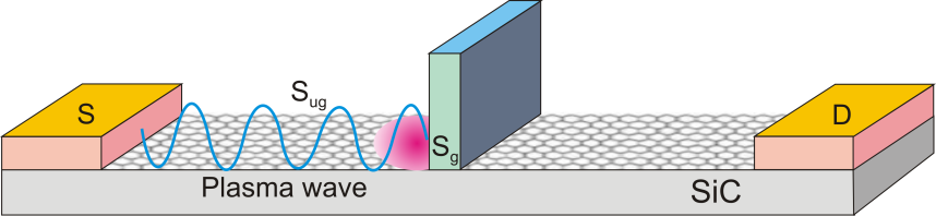
Fig. 4. The detection mechanism in graphene THz FET photodetector.
The temperature gradient in the detector area generates an internal voltage responsible for the current. It can be determined using the formula:

where αS is the Seebeck coefficient commonly expressed in μV/K. The Seebeck coefficient is usually expressed by:

where σ is the conductivity of the material [8], and k is the Boltzmann constant. The derivative of the electrical conductivity σ with respect to energy E must be evaluated at the Fermi energy [E = EF = ħvFkF; here: ħ is the reduced Planck constant, vF is the Fermi velocity (in graphene about 106 m/s), and kF is the Fermi wavevector]. The sign of the Seebeck coefficient is determined by the majority charge polarity in the semiconductor.
In the case of two different conductors “a” and “b”, electrically connected by a single set of their ends, the coefficient αS is the effective or relative Seebeck coefficient. Then the thermovoltage is equal to:

where αa and αb are the absolute Seebeck coefficients of the materials a and b.
In the case of two junctions between the contact metal and the semiconductor, the voltage difference across them is:

In (4), the term αSmetal is neglected. It turns out that the Seebeck coefficients of pure metals are in the order of 1 µV/K, much smaller than typical values for semiconductors.
Figure 5 presents the Seebeck coefficients as a function of resistivity for various materials. As shown, the magnitude of ΔVPTE is small, typically ranging from tens of µV to tens of mV. In such a situation, ohmic contacts to the semiconductors are necessary. When illuminating a homogeneous semiconductor, a weak temperature gradient can be achieved if no current flows in the device (i.e., no external bias voltage is applied). It is worth noting that both relative and absolute Seebeck coefficients depend on temperature and the proportionality between the generated potential difference and the temperature gradient holds only over a small temperature range.
It is essential to distinguish between the PTE and the bolometric effect. In the latter case, temperature changes affect the material resistivity. The bolometric effect does not create current in the device; it only modifies the current value under the influence of external voltage and illumination. In the case of a bolometer, the direction of the photocurrent is related to the change in the material conductivity with temperature, while in the case of a PTE, the direction of the photocurrent is related to the difference in the Seebeck coefficients between the junction components.
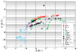
Fig. 5. The Seebeck coefficients as a function of resistivity for various materials (after [9]).
PTE plays an important role in the photocurrent generation in LDS detectors [3, 10]. Consider graphene as an example. In graphene, due to the high energy of optical phonons (~ 200 meV), hot carriers created by light remain at a temperature higher than the lattice temperature for many picoseconds. Therefore, equilibrium between hot electrons and the lattice is achieved by a slower scattering process between charge carriers and acoustic phonons (nanosecond range). The heat capacity of the carriers is significantly smaller than that of the lattice, resulting in a larger temperature gradient within the material and thereby enhancing the PTE effect. Figure 6 further illustrates this process. The light spot induces temperature changes in the carriers and the hot carriers generated by the photons diffuse under the influence of the temperature gradient, leading to photocurrent generation (since the carriers and the lattice have different temperatures). The direction of the photocurrent resulting from the photovoltaic (PV) and PTE effects is the same, making it difficult to experimentally determine their relative contributions.
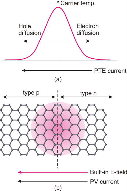
Fig. 6. The mechanism of a PV current generation in a graphene p-n junction: (a) the effect of light intensity distribution on the carrier concentration profile; (b) the PTE effect generating PV current flow from the n-type region to the p-type region, and the built-in electric field of the p-n junction (adapted after [10]).
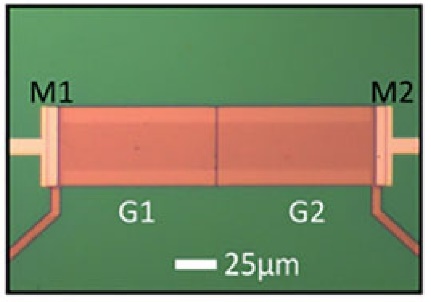
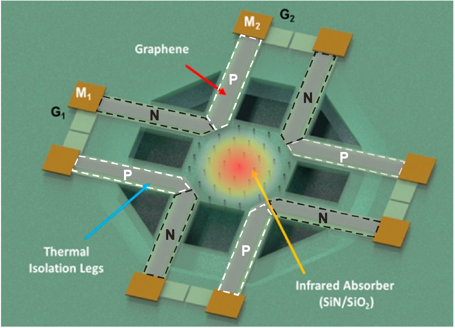
Figure 7 illustrates the structure of a thermoelectric graphene photodetector [9]. The detector is constructed by combining PTE graphene detectors with silicon nitride micromachined membranes. The device, consisting of a graphene sheet with double split back gates, generates a PV voltage across electrodes M1–M2 depending on the voltage applied to the back gates. The thermoelectric effect is observed even at 10.6 μm. According to (3): ΔV = (αp − αn)Δ T, where (αp − αn) is the difference of the Seebeck coefficient between the p- and n-regions of graphene, and Δ T is the temperature difference between the graphene p-n junction and the metal contacts.
As shown in Fig. 7(c), multiple graphene photodetectors are connected in a thermopile consisting of an IR absorber suspended on a substrate, a series of thermal arms connecting the absorber to the environment, and interleaved

(a)
(b)
(c)
Fig. 7. Graphene thermopile: (a) diagram of a thermopile with a split gate and substrate, (b) its microscopic image. M1 and M2 denote metal contacts with graphene, while G1 and G2 denote split gates that electrostatically dope the graphene channel, thereby forming a p-n junction, (c) diagram of the device and its optical image. The white and black areas represent graphene with p-type and n-type conductivity, respectively, and the square in the middle serves as a dielectric absorber. The entire structure is suspended on a substrate to reduce vertical thermal conductivity (after [9]).
p- and n-type graphene channels on top. The heating absorber is a dielectric multilayer thin film that is electrically probed by graphene p-n junctions. Thanks to the use of an optimised IR radiation-absorbing layer made of a combination of SiO2/Si3N4/SiO2 deposited by plasmaenhanced chemical vapour deposition (PECVD), absorption in the 8–12 μm spectral range exceeded 40%. The freestanding absorbing membrane was fabricated by isotropic XeF2 etching to undercut the underlying silicon.
If the thermopile detectivity is limited by Johnson noise, then D*2/τ (where τ is the response time) can be expressed by [9]:

In (5), the first term (αabs/t) is the absorbance per thickness, t indicating the capability of IR absorption. The second term Δαs2/ρ2D with 2D resistivity of graphene is determined by the electrical and thermoelectric properties of the sensing material. In fact, the Δαs2/ρ2D term is the thermoelectric figure of merit (FOM) for thermopile IR detectors. The third term 1/κthcv determines the quality of thermal isolation. Here, κth is the thermal conductivity of the absorber (heat transport factor), and cv is the specific heat capacity. Equation (5) is independent of the lateral geometry.
The Seebeck coefficient as a function of resistivity for various 2D and 3D materials is shown in Fig. 8. For comparison purposes, the FOM graph is shown as a function of resistivity. As shown, the FOM coefficient for standard CVD graphene on SiO2, with a mobility of 2000 cm²/Vs, exceeds that of all metal thermocouples and most thermoelectric materials. It can be assumed that the use of higher-quality graphene and appropriate passivation will yield an FOM that is two orders of magnitude higher than that of other material systems [9]. It should also be noted that the FOM of 2D transition metal dichalcogenides (TMDs) is higher than that of their 3D counterparts, indicating their great potential in heat detection and other thermoelectric applications.
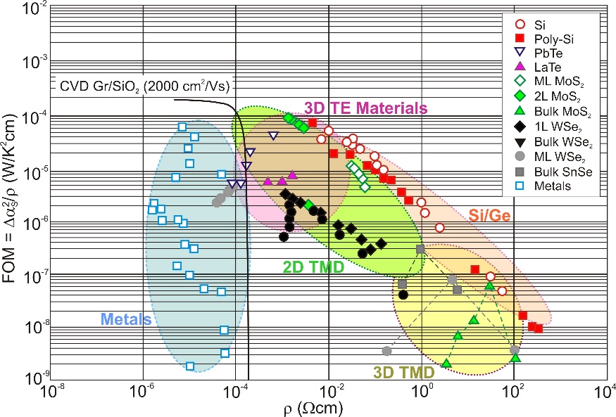
Fig. 8. The thermoelectric figure of merit (FOM) as a function of resistivity for various materials (after [10]).
Figure 9 compares the detectivity and response speed of a graphene thermocouple with various thermal detectors, including bolometers (VOx, etc.), thermocouples (poly-Si, Al, and other thermoelectric materials), and pyroelectric detectors (PZT and other piezoelectric materials). For more advanced thermal detectors, the detectivity at room temperature is approximately 108 –109 cmHz1/2/W. As shown in Fig. 9, the performance of graphene thermocouples is significantly lower than that of commercial thermal detectors, with a value below 106 cmHz1/2/W. However, the theoretically estimated sensitivity is even better than that of standard 3D technologies available on the global market. For example, a 10 nm thick graphene nanophotonic absorber with good mechanical stability and 50% absorption, could outperform any existing bolometer.
Recently, a compact thermoelectric photodetector based on resonantly coupling MWIR radiation with a Sb2Te3-Bi2Te3 thermoelectric junction has been presented [11]. Sb2Te3 and Bi2Te3 are chalcogenide materials, with small bandgaps in the range of 0.1–0.3 eV [12]. Both semiconductors have absolute Seebeck coefficients in the range of 100–200 μV/K, electrical conductivities of ≈ 105 S/m, and thermal conductivities of ≈ 1 W/mK [13]. Since Sb2Te3 is a p-type and Bi2Te3 is an n-type semiconductor, with negative and positive Seebeck
Fig. 9. Detectivity as a function of response time for various graphene thermopile architectures compared to popular uncooled IR detectors (after [10]).
a thermocouple pair for thermoelectric conversion. Reducing the cross-sectional dimensions of thermoelectric electrodes significantly reduces phonon thermal conductivity while maintaining the thermoelectric power factor. This effect has become an effective method for improving the performance of thermoelectric devices.
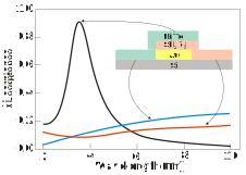
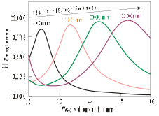
The PTE detector is based on intrinsic optical absorption in Bi2Te3 and Sb2Te3, along with an asymmetric FabryPérot-like resonance structure, as illustrated in Fig. 10(a). The device design eliminates the need for membranes, simplifying production and improving scalability. Incident light is reflected and transmitted in the thermoelectric leads but is strongly absorbed and converted into heat in the p-n thermoelectric junction. The temperature gradient created in the devices generates the Seebeck voltage. By modulating the size of the optical resonator, the optimal detection wavelength can be tuned, as shown in Fig. 10(b) and (c).
(a)
(b)
(c)
Fig. 10. Bi2Te3-Sb2Te3 thermoelectric detector: (a) principle of operation, (b) and (c) simulated absorption spectra for devices with diverse structures and varied resonance thicknesses (after [11]).
It should be noted that tuning the wavelength in the LWIR range requires increasing the material thickness to increase the resonator thickness. This increases the device thermal capacity, thereby reducing the detector response speed.
The Bi2Te3 and Sb2Te3 films were deposited on glass and silicon substrates by magnetron sputtering. The RMS roughness of films about 1.5 nm was significantly smaller than the wavelengths of light being detected (> 2 μm). The estimated detectivity limited by Johnson noise was 3.2 · 106 cmHz1/2/W; the responsivity value was 10.2 V/W at resonance, and the bandwidth was on the order of 1 kHz. The detectivity is lower than that of commercial thermoelectric detectors (typically in the range of 108 cmHz1/2/W). However, commercial detectors are typically manufactured on suspended membranes in airevacuated environments, which provides maximum thermal insulation. It can be expected that comparable detectivities can be achieved under similar thermal conditions.
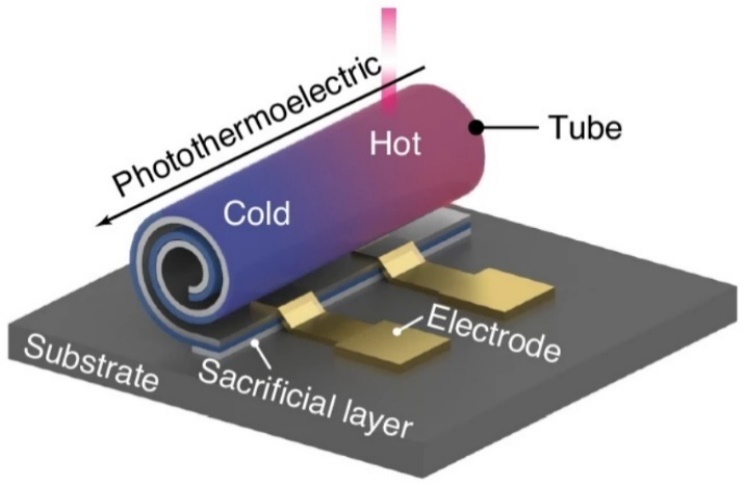
To enhance localised light absorption in detectors, optical absorbers such as antennas, plasmonic nanostructures, and metamaterials are used. Localising energy in 3D micro- and nanostructures can effectively enhance PTE energy conversion. Self-rolling structures are not used as optical microcavities to confine electromagnetic field energy [14]. This idea of detector design was implemented by Huang et al. [15], who fabricated a self-rolled tubular Te-based detector (TTD) with enhanced PTE effect and sensitivity. The tubular structure is an excellent optical absorber due to the light-trapping effect inside the tube wall.
The core of the detector is a multilayer, self-folding tubular structure (consisting of a polycrystalline Te layer, a pre-strained layer, and a protective layer) – see Fig. 11(a). The detector also comprises electrodes, a sacrificial layer, and a substrate. Aluminium oxide (Al2O3) serves as the protective layer, palladium (Pd)/gold (Au) as electrodes, silicon nitride (SiNx) as the pre-strained layer, germanium (Ge) as the sacrificial layer, and a thermally oxidised silicon wafer as the substrate. The final TTD shape was fabricated by selectively etching the sacrificial layer and self-rolling a tabular structure driven by a stress gradient within the SiNx layer.
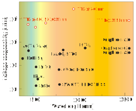
Figure 11(b) compares the voltage responsivity of TTD with other photodetectors based on the PTE effect. As shown, the TTD detector exhibits higher broadband sensitivity than other PTE detectors made from various materials, both inorganic and organic materials. TTD achieves the highest voltage sensitivity of 252.13 V/W and a detectivity of 1.48 · 1011 cmHz1/2/W for laser radiation at 940 nm. This self-rolled detector structure effectively localises optical and thermal energy, ensuring high photodetection efficiency. Additionally, tube detectors are considered the optimal platform for identifying light polarisation. The unique 3D geometry and anisotropy of the detector provide polarisation sensitivity. The experimental results shown in Figs. 12(a)–(c) indicate that increasing the polarisation angle of incident light at various wavelengths causes the photovoltaic voltage to oscillate periodically. The polarisation-resolved photovoltaic voltage can be well fitted to a sine function. The calculated TTD dichroic coefficients for lasers emitting at 940, 1550, and 635 nm are 1.20, 1.21, and 1.19, respectively. It can be concluded that integrating functional materials with 3D on-chip
(a)
(b)
Fig. 11. Self-rolled tellurium photodetector: (a) schematic detector operation diagram and its components, (b) comparison of the voltage responsivity of TTD with other self-driven PTE photodetectors (after [15]).
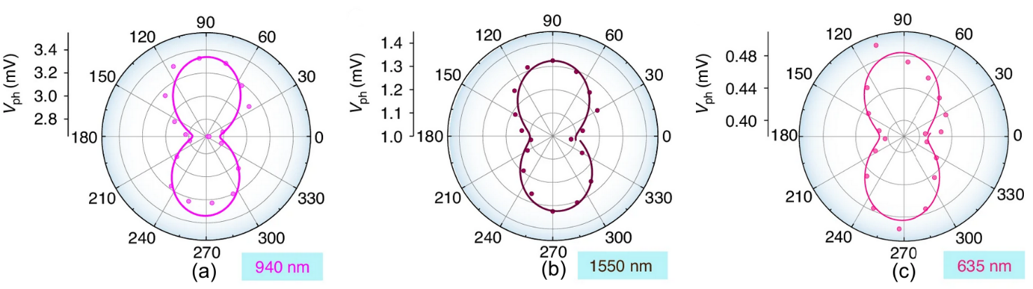
Fig. 12. Polarisation detection of TTD. Figures (a) and (c) show polar plots of measured photovoltage under polarised light of 940, 1550, and 635 nm lasers (after [15]).
detectors will lead to the development of even more technologically advanced detectors in the future.
In contrast to traditional thermoelectrics, which rely on bulk material properties, nanothermoelectrics use various combinations of nanofabrication and material synthesis techniques to design charge carriers and/or phonon transport, thereby enhancing thermoelectric performance. Varpula et al. have demonstrated an uncooled high sensitivity thermoelectric thermal detector based on suspended 40 nm thick single-crystalline silicon thermocouples [16]. This device is micromachined using standard silicon and aluminium materials, which provides an attractive procedure for monolithic integration with CMOS readout circuits.
One example of a detector design is shown in Fig. 13. On the right, a pair of heavily doped n-type and p-type silicon beams acts as a thermocouple and supports a 40 nm thick silicon membrane. On the left side, a pair of heavily doped silicon beams provides an electrical connection for a meandering doped silicon heating resistor arranged in the silicon membrane. An aluminium layer provides a lowresistance electrical contact between the n-type and p-typedoped thermocouple areas. The detector consists of a 110 × 110 µ m2 membrane suspended on four beams 190 µ m long and 8 µ m wide. The highly doped silicon thermocouple is connected to the membrane by a lowconductivity aluminium contact with a contact resistance of 2.8 Ω. The detector exhibits a noise-equivalent power of 13 pW/Hz1/2 and a thermal time constant of 2.5 ms.
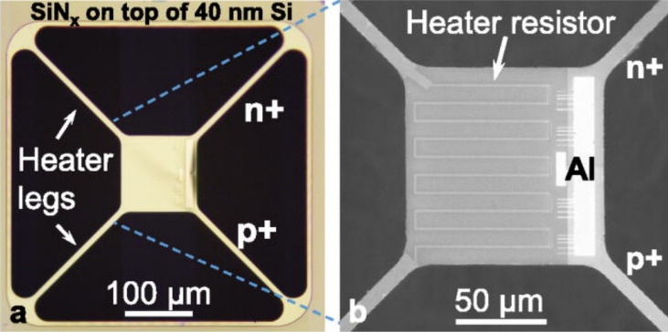
Fig. 13. Optical and scanning electron microscopy images of the Si nanomembrane thermal detector (after [16]).
Further evolution of nanothermoelectric and nanomembrane thermal detectors has been proposed by scientists from VTT Technical Research Centre of Finland Ltd. [17–19]. In these devices, the signal is generated by the thermoelectric effect, providing advantages over resistive bolometers, i.e., fewer noise sources and zero power consumption in the detector itself.
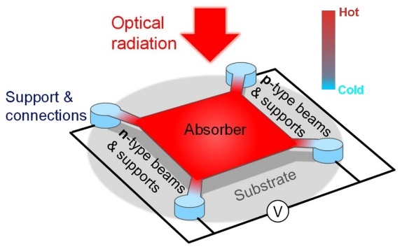
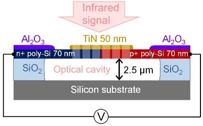
Figure 14(a) shows a schematic diagram of a thermoelectric bolometer. The device comprises an optical absorber, thermoelectric converter (utilizing p-type and n‑type thermoelectric materials), supporting structure, electrical contacts, and readout electronics. As a result of incident radiation, a temperature gradient is created along the structure supporting the absorber. This gradient, in turn, generates an electrical voltage in the p-type and n-type thermoelectric materials (i.e., legs) located in/on the supporting structure. The generated thermoelectric voltage serves as the input signal for the readout electronics located in the substrate. To increase the absorption of IR radiation, a quarter-wave nanomembrane resistive absorber is employed.
(a)
(b)
(c)
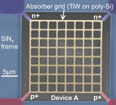
Fig. 14. Thermoelectric bolometer: (a) schematic design structure supported by four beams (two beams are also common), (b) scanning electron picture, and (c) a cross-sectional schematic of the detector with the same supporting beam dimensions and varying absorber grid linewidth and pitch (after [17] and [18]).
The practical design of the detector is illustrated in Figs. 14(b) and (c). The absorber is suspended above the optical cavity by means of 70 nm thick p-type and n-type poly-Si beams, which form two thermocouples. The strains in the poly-Si beams are regulated by a 50 nm thick Al2O3 deformation compensation frame. The thermocouple pairs are electrically connected by a 50 nm thick TiN metal layer. This layer also acts as an absorbing element. The metalpolysilicon structure of the absorber is arranged in a grid pattern, allowing for the selective removal of the oxide substrate during fabrication and the tuning of the absorber optical impedance. The absorber grid is suspended above an optical cavity. The depth of the optical cavity is 2.5 μm and has been selected to match the thermal radiation at room temperature with a wavelength of 10 μm.
The devices with absorber areas between 24 × 24 μm² and 25 × 25 μm² have thermal time constants in the range of 190 μs to 208 μs, which are significantly shorter than the typical time constants observed for resistive bolometers (above 1 ms). Thermal time constants are proportional to the thermal mass of the absorber, which is the total area occupied by the absorber grid material. The detector responsivities and detectivities are in the ranges of 334– 494 V/W and (7.9–8.7) · 107 cmHz1/2/W, respectively [19].
Further optimisation of nanothermoelectronic bolometer resistance and optical absorption efficiency is expected to lead to the achievement of D* = 8.3 · 10⁸ cmHz1/2/W while maintaining response speed [18, 19]. The above data indicate the great potential of this type of bolometer for the development of fast, sensitive, uncooled IR detectors.
4. Nanoelectromechanical resonator detectors
The sensitivity of room-temperature thermal detectors remains significantly below the fundamental detection threshold set by the detectivity D* = 1.8 · 1010 cmHz1/2/W. This value is given by temperature fluctuations of both the detector and its surrounding environment [6]. Thermoelectric detectors are typically limited by electronic noise, such as Johnson noise or 1/ f noise. To overcome the existing limitations of thermal detectors, alternative detection mechanisms have been explored. One of the new approaches is a temperature-sensitive mechanical resonator.
In an electromechanical detector, incident radiation induces a temperature change in the suspended resonator. Temperature changes alter the resonator mechanical properties, especially its resonant frequency, which is electronically detected. The change in frequency is directly proportional to the amount of radiation absorbed, allowing for high detector sensitivity.
The first mention of a mechanical IR detector appeared in 1969 in Cary’s patent [20]. This macroscopic resonator, featuring a tensioned film, serves as a temperature-sensing element. In 2011, it was first demonstrated as a nanometerthin tensioned metal and a SiN foil resonator element for temperature sensing [21]. Later in 2013, concepts based on tensioned SiN strings were introduced [22, 23]. Recently, nanoelectromechanical resonators have been further developed using various designs – examples of their construction are shown in Fig. 15.
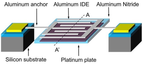
Over the past decade, nanomechanical photothermal sensors have emerged as a crucial tool for radiation detection due to their exceptional temperature sensitivity. One of these new technologies is an AlN nanoplate resonator. It shows great potential, competitive with the currently dominant microbolometers. Their basic element is a resonator with a transverse stretching mode [see Fig. 15(a)]. The resonator consists of a 50 nm thick AlN piezoelectric layer placed between a 30 nm thick Al finger electrode and a 20 nm thick platinum (Pt) plate. The device demonstrates ultrafast time constant (τ ∼ 166 μs) and high sensitivity (noise equivalent power , NEP ∼ 549 pW/Hz1/2) [24].
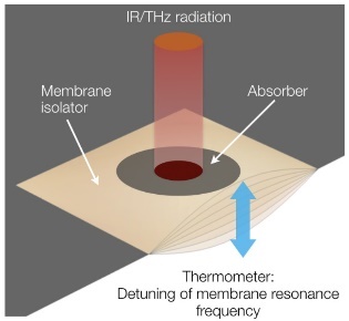
Figure 15(b) shows an uncooled IR detector consisting of a 1×1 mm² nanoelectromechanical drum resonator made of 50 nm thick, low-stress SiN [25]. Conventional UV lithography was used to fabricate it and metal electrodes (Cr/Au = 5 nm/100 nm) were deposited by physical vapour deposition, using chromium as an adhesive layer. The SiN drum was fabricated on the rear side by reactive-ion etching and a potassium hydroxide (KOH) etching. Finally, a thin absorbent layer approximately 14 nm thick was applied to the back side. The detector operates on the principle of thermally inducing a detuning of the resonance frequency.
(a)
(b)
(c)
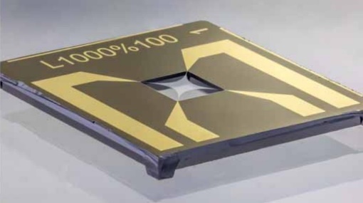
Fig. 15. Examples of nanoelectromechanical resonator designs: (a) schematic diagram of an AlN nanoplate resonator with nanoscale metallic (Al) anchors (after [24]), (b) drum resonator made of a 50 nm thick low-stress SiN (after [25]), and (c) trampoline resonator sample made of SiN with gold electrodes (after [26]).
A broadband absorber provided sensitivity in the range from 5 μm to 20 μm with a NEP of 320 pW/Hz1/2.
The best performance has been demonstrated for trampoline nanoelectromechanical thermal detectors. Compared to a drum, a trampoline has enhanced thermal responsivity due to a better thermal isolation of the central detection area [26]. The resonator shown in Fig. 15(c) is made of a thin layer of SiN rich in silicon with low stress and a thickness of 50 nm. This layer was produced by a low-pressure chemical vapour deposition. The 5 μm-wide trampoline strips are supported by a 380 μm thick silicon frame. The chips measure 5 × 5 mm, while the frame size is 1 × 1 mm. Gold electrode contacts with a width of 1 μm and a thickness of 190 nm are deposited by thermal evaporation onto previously deposited 10 nm thick chromium adhesive layers.
The developed trampoline resonator exhibits excellent performance [26, 27]. Compared to other SiN nanomechanical resonators used as IR detectors with NEP values in the range of hundreds of pW/Hz1/2, this parameter could be improved by two orders of magnitude with a minimum measured value of 7 pW/Hz1/2. In addition, the response time of the trampoline detector is improved by a factor of 3 compared to drum SiN detectors and for the smallest trampolines, it is 4 ms. The detector thin-film absorber exhibits a spectrally flat 50% absorption over the entire mid-IR spectral range from 1 to 25 μm.
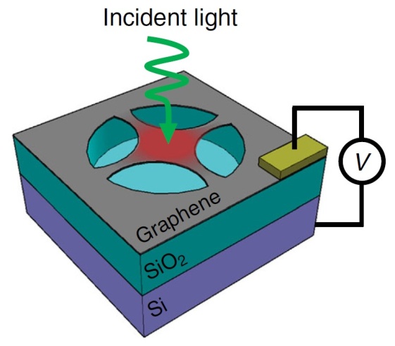
Blaikie et al. [28] also demonstrated nanoelectromechanical graphene systems – see Fig. 16, in which absorbed light heats a suspended graphene resonator while inducing thermal tensions within it. Changes in stress in the resonator modulate its resonant frequency. A schematic design of the resonator with a suspended graphene membrane is shown in Fig. 16(a). The nanomechanical graphene bolometer (GNB) was fabricated by transferring graphene onto a Si/SiO2 substrate with patterned holes, enabling the creation of circular drum resonators. Some membranes have a trampoline-like shape, achieved by using a focused ion beam technique. The most sensitive device has a built-in trampoline with a diameter of 6 μm and tethers 200 nm wide. To set the graphene resonators in motion, an a.c. voltage is applied between the graphene and the back gate.
As a result of light absorption, the temperature of the membrane increases, and the resulting thermomechanical
(a)
(b)
(c)
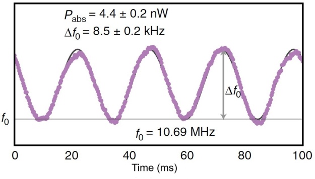
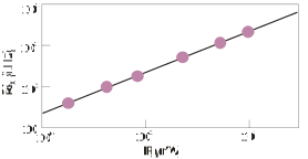
Fig. 16. Nanomechanical graphene resonator: (a) structure, (b) mechanical resonance frequency as a function of time for a trampoline with a diameter of 8 μm and tethers with a width of 500 nm. The power of the incident radiation modulated at a frequency of 40 Hz was 190 nW, (c) measured change in resonance frequency as a function of absorbed power. Absorbed power of 4.4 nW causes a frequency change of Δ f0 = 8.5 kHz (after [28]).
stresses cause the resonance frequency to shift by a value of [28]:

where α is the thermal expansion coefficient, ν is the Poisson ratio, σ0 is the initial in-plane stress, Y is the 2D elastic modulus, f0 is the initial frequency, and Δ T is the temperature change. For typical nanomechanical graphene resonators, a full line-width shift requires Δ T ~ 100 mK, a value that can be easily measured.
Figures 16(b) and (c) show the frequency sensitivity to light absorption by recording the f0 time when sinusoidally modulated light with a power of 4.4 nW is incident on the GNB. The best-fit line to these data indicates a resonance shift of 2.3 kHz/nW.
The GNB detector achieved a sensitivity of 2 pW/Hz1/2 and a bandwidth of up to 1 MHz, demonstrating previously unattainable performance at room temperature and significantly exceeding the response speed of state-of-the-art ‑ bolometers operating at room temperature (i.e., e deposition process above 300 °C and integrated circuit compatibility).
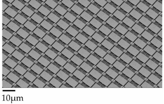
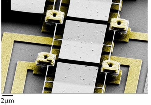
Duraffourg et al. provided the first demonstration of 12 μm pitch nanoelectromechanical resonant IR sensors with fully integrated capacitive transduction [29, 30]. This array was manufactured using a low-temperature fabrication process derived from classical bolometers. The detailed procedure of their fabrication is described in [29]. Figure 17(a) presents a scanning electron microscopy (SEM) image of the matrix of microelectromechanical pixels, whereas Figure 17(b) presents the H-shaped single pixel.
The resonance the frequency shift Δ f of a electromechanical detector is equal [29] to:

where Pin denotes the incident optical power, Rf is the sensitivity dependent on both the thermal conductivity of the paddle insulation (through the insulating legs), τth = C / Gth is the thermal time constant, C is the thermal conductivity, αf is the temperature frequency coefficient, f0 is the resonance frequency, β is the detector fill factor (for arrays), and ω is the circular frequency. Thermal conductivity is primarily determined by the legs thermal conductivity.
Electromechanical resonators with H-shaped pixels (nanorods with a length of 9 µm and a cross-section of 250 × 30 nm²) were characterised by a NEP value of 140 pW and a response time of less than 1 ms. These parameters exceed those achieved for standard bolometers with small α-Si and VOx pixels [31].
As a figure of merit (FOM),

is usually introduced to evaluate the quality of a microbolometer technology, where NEDT is the noise equivalent difference temperature. The NEDT of 2 K at 50 Hz, with a sub-millisecond response time, was extracted for incident radiation in the 8–12 μm range. Then FOM is approximately 2 K·ms in comparison with 0.5 K·ms for standard bolometers.
(a)
(b)
Fig. 17. Scanning electron microscopy (SEM) pictures of an array of electromechanical pixels: (a) zoom‐in on the center of the 96 × 96 array, (b) SEM picture of a typical H‐shape pixel ‒ nanorod length = 1.5 μm, width = 250 nm, and thickness = 180 nm (insulation arm length = 8.6 μm) (after [29]).
5. Bolometers
The responsivity of the bolometer is described by [31]:

where Ib is the current bias, α is the temperature coefficient of resistance (TCR), R is the resistance of the bolometer, η is the absorbance of the sensitive region , G is the thermal conductance, ω is the angular frequency of modulation of the radiation, and τ is the thermal response time. Equation (9) indicates that responsivity is inversely proportional to thermal conductivity (G) and directly proportional to TCR. Furthermore, responsivity is a function of bias voltage, operating frequency, and wavelength.
Microbolometer materials must meet the following key requirements:
-
low thermal conductivity (G),
-
low noise, and
-
high TCR (α),
-
compatibility with silicon (Si) integrated circuit (IC) fabrication processes.
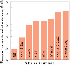
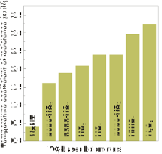
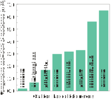
Currently, these features are achieved using several materials. Most of the uncooled microbolometer technology is dominated by conventional materials, like VOx and amorphous α-Si, in terms of performance and large-scale production. Their TCR values at room temperature are typically: 3%/K for α-Si, 2.4%/K for VOx, and 2.6%/K for newly emerged and developed TiO2 thin films [32]. Additionally, metals such as Ti and Pt, as well as emerging carbon-based materials, including carbon nanotubes (CNTs) and graphene, are compatible with CMOS silicon technology. The comparison of TCR results between various uncooled microbolometers is presented in Fig. 18. To achieve better thermal insulation and minimise heat loss, various manufacturing techniques and architectures have been proposed. These modifications also affect TCR values.
Graphene (the material with the highest mass per unit area of all known materials) exhibits exceptional thermal stability and spectral absorption. These properties make graphene a useful active bolometric absorber. However, due to the weak temperature dependence of electrical resistivity, graphene has not challenged the dominance of thermal detectors in the global market.
(a)
(b)
(c)
Fig. 18. Comparison of temperature coefficient of resistance values for various bolometric materials: (a) Si-based materials, (b) VOx-based materials, and (c) carbonbased materials (after [32]).
Among the new generation of materials useful for microbolometer design, CNTs stand out for their properties [33]: high optical absorption, low thermal capacity, and high response speed. However, these materials are still in the development phase of technological refinement. Common methods for synthesising CNTs include CVD, laser ablation, and arc discharge. Deposition from presynthesised materials is also possible, using techniques such as electrophoretic deposition (EPD) and wet deposition methods. The choice of method depends on the application; for example, whether the goal is to deposit nanotubes on a substrate or transfer them to another substrate.
Various types of CNTs are used. The most important are single-walled carbon nanotubes (SWCNTs) and multiwalled carbon nanotubes (MWCNTs). Double-walled carbon nanotubes (DWCNTs), consisting of two nanotubes embedded within each other, are also popular. Various types of CNTs have been developed, each with distinct characteristics. Modifications to their chemical composition and structure enhance the specific properties required for specific applications. For example, for bolometers, one of the most important parameters is TCR. Figure 18(c) demonstrates the effect of modifying the material type on this parameter. At the current state of carbon nanotube technology, the performance of bolometers manufactured with their use is inferior to commercial, standard a-Si and VOx bolometers – their typical detectivity is 106 − 107 cmHz1/2/W at room temperature [32].
One of the primary trends in imaging system development is reducing the system size, weight, and power consumption (SWaP), with the ultimate goal of lowering system costs. This SWaP criterion also influences the reduction in sensor pixel sizes. Reducing pixel size is also desirable to improve the resolution and reliability of the imaging system. The optimal pixel size in LWIR is expected to be 5 µ m. Researchers from Duisburg (Fraunhofer IMS) have proposed achieving this goal by modifying the bolometer structure.
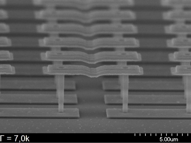
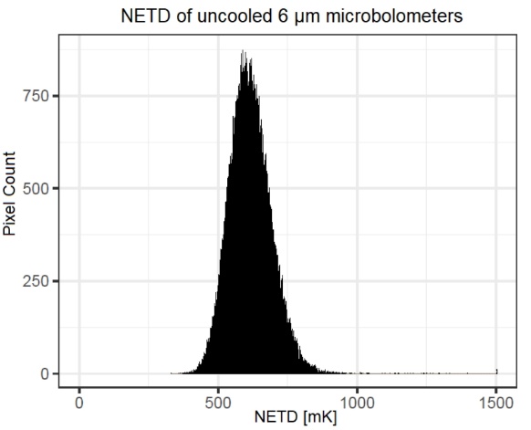
The nanotube-microbolometers are composed of an IR-sensitive membrane with two vertical nanotubes serving as electrical contacts, which are connected to the readout integrated circuit. The common design and concept ideas are presented in [34] and [35]. SEM images of the microbolometers are shown in Fig. 19(a). The Fraunhofer IMS team thus introduced the first uncooled thermal imager based on microbolometers with a 6 µm pixel size. The main parameter characterising the imaging system, called NEDT, was 611 mK [see Fig. 19(b)], which was below the level of available commercial cameras (typically 30–50 mK). However, the functionality of such a device was demonstrated for the first time, and the potential for further improvement was identified.
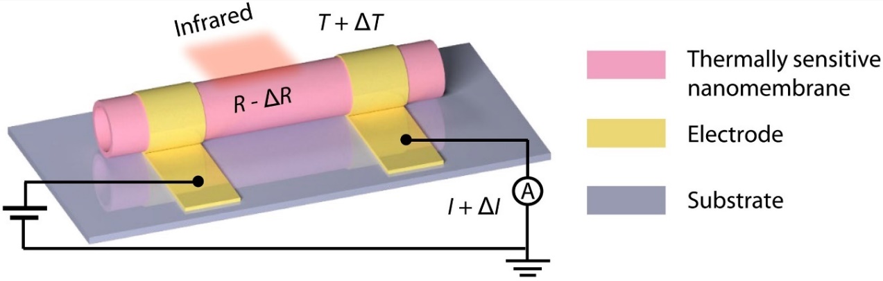
Recently, a sensitive tubular VO2 bolometer fabricated using a one-step rolling process has been demonstrated [36]. This method of fabricating bolometers was achieved by combining existing integrated circuit manufacturing techniques, enabling the transformation of flat VO2 nanomembranes into microtubes with a 3D cylindrical cavity geometry – see Fig. 20(a). In the optimal case, the contact between the tube and the plane is aligned, thereby significantly reducing heat conduction between the two. In this way, the tubular device provides better thermal insulation while occupying significantly less chip area.
(a)
(b)
Fig. 19. Nanotube-microbolometers: (a) daisy chain of nanotube contacts (after [29]) and (b) NEDT of an uncooled thermal imager with a 6 µm pixel size on a 17 µm QVGA-ROIC (after [35]).
Additionally, this tubular microcavity structure enhances light coupling to the detector by trapping it within the tube wall, thereby improving the absorption of incident radiation.
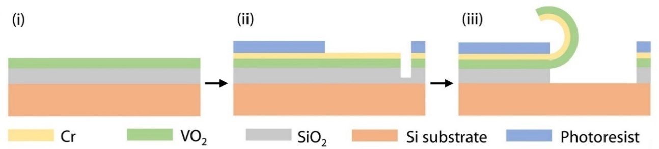
Figure 20(b) presents a schematic of the preparation process for a VO2 microtube. The VO2 nanomembrane, with a thickness of ~ 60 nm, was sputtered onto a 4-inch silicon wafer coated with a 500 nm thermal SiO2. After growing the 40 nm Cr layer on VO2, a portion of VO2 is removed by reactive ion etching (RIE) to create an etching window. Next, through photolithography, only the VO2 nanomembranes and the etching window are exposed. Subsequently, the SiO2 layer was selectively etched, and the VO2/Cr layer was released from the substrate and rolled up into a tubular structure driven by the strain gradient.
The bolometer made in the above manner is characterised by a detectivity of ~ 2 · 108 cmHz1/2/W in the wide IR band, a response time of ~ 2.0 ms, and a calculated noise equivalent temperature difference of 64.5 mK.
6. CMOS-compatible pyroelectric detectors
Pyroelectric detectors are widely used due to their simple design, robustness, and good performance. In most detectors, the active regions are thin layers of single-crystal lithium tantalate (LT) or pyroelectric lead zirconate titanate (PZT) deposited on a silicon substrate. Actually, an interesting direction of research are pyroelectric materials [such as aluminium nitride (AlN), gallium nitride (GaN),
(a)
(b)
Fig. 20. VO2 tubular bolometers: (a) 3D architecture of the working principle of tubular bolometers and (b) schematic illustrating the preparation process of VO2 microtube (after [36]).
zinc oxide (ZnO), and doped hafnium oxide (HfO2)], which offer the potential to fabricate devices fully compatible with CMOS technology on large silicon wafers. It turns out that the pyroelectric coefficient of materials compatible with silicon CMOS is comparable to that of crystalline pyroelectric materials, including triglycine sulfate (TGS), lithium tantalate (LiTaO3), lithium niobate (LiNbO3), and various ceramic materials [37].
The polarisation changes Δ Ps, due to a change in temperature Δ T is described by:

where p is the pyroelectric coefficient. Plot of the spontaneous polarisation and pyroelectric coefficient vs. temperature is given in Fig. 21.
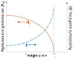
Fig. 21. Dependence of spontaneous polarisation and pyroelectric coefficient on temperature. ).
The comparison of the pyroelectric performance of CMOS-compatible materials with the single crystal and ceramics-based materials is summarised in Table 2. In the active region of the detector, materials with a low dielectric constant, low dielectric loss, high pyroelectric coefficient, and low volume-specific heat are preferred. Therefore, three FOMs are distinguished, which are derived from the pyroelectric coefficient:
- for high current responsivity:

- for high voltage responsivity:

- for high detectivity:

where Cv is the volume specific heat capacity, ε’ is the real and ε” is the imaginary part of the dielectric constant of the pyroelectric material.
It is well known that the CMOS-compatible detectors provide a low-cost approach for IR imaging applications. The fabrication of the CMOS-compatible IR arrays is based on the combination of the standard CMOS process and a simple post-CMOS micro-electro-mechanical system (MEMS) process. The concept for the fully integrated CMOS-compatible pyroelectric detector is illustrated in Fig. 22. The detector comprises two electrodes: a lower electrode fabricated from phosphorus-doped polysilicon and an upper electrode made of AlSiCu (1 μm thick). Both electrodes are equipped with the necessary contact pads. Between these electrodes is an active layer of the detector, made of AlN. The lower polysilicon electrode also acts as an absorber of incident radiation. Absorbed radiation alters the temperature in both the polysilicon and AlN layers. To ensure that the detector active area is isolated from its substrate (which is crucial for efficient operation), the detector is placed on a free-standing Si3N4 (140 nm thick)/SiO2 (2 µm thick) membrane.
Among the tested devices, the highest sensitivities were achieved with detector areas of 0.25 mm² and 0.50 mm², and a membrane size of 1.44 mm² [38]. The noise equivalent power (NEP) of the first detector was 5.3 · 109 W/Hz1/2, corresponding to a detectivity of 9.4 · 106 cmHz1/2/W. The performance of the demonstrated devices does not yet match that of commercially available pyroelectric devices, which typically achieve a sensitivity of about 108 cmHz1/2/W.
Properties of pyroelectric CMOS-compatible materials, the single crystal, and ceramics-based materials (after [37]).
| Material | Tc (°C) | εr | p (μC/m2K) | Fi (10−10 mV−1) | Fv (m2/C) | FD (10−5 Pa−1/2) | tanδ |
|---|---|---|---|---|---|---|---|
| TGS | 49 | 40 | 350 | 1.35 | 0.38 | 4.5 | 0.025 |
| DTGS | 61 | 33 | 400 | 1.67 | 0.57 | 6.9 | 0.020 |
| TGFB | 73 | 50 | 400 | 1.54 | 0.35 | 4.4 | 0.028 |
| LATGS | 49 | 35 | 330 | 1.32 | 0.43 | 7.5 | 0.010 |
| LiTaO3 | 665 | 47 | 190 | 0.59 | 0.14 | 4.1 | 0.005 |
| LiNbO3 | 1210 | 31 | 96 | 0.35 | 0.14 | – | – |
| PbTiO3 | 460 | 190 | 180 | 0.56 | 0.033 | – | – |
| PbZrO3 | 200 | 250 | 350 | 1.35 | 0.061 | 4.05 | 0.005 |
| PZT | 315 | 471 | 350 | 1.09 | 0.026 | 2.40 | 0.005 |
| Mn:PZT | 118 | 196 | 316 | – | 0.073 | 4.33 | 0.014 |
| GaN | 9.5 | 4.4–12.4 | – | – | – | – | |
| AlN | 2000 | 8.5 | 6–33 | 0.03 | – | 0.48–2.4 | 0.005 |
| Sc:AlN | – | 8.35–20 | – | – | – | – | |
| Si:HfO2 | – | 26 | −46.2–84 | 17.55 | 0.062 | 6.19 | 0.08–0.1 |
| Zr:HfO2 | – | 24.5 | 1.5–47.8 | 0.01–0.22 | 0.02–0.10 | 0.2–12.5 | 0.008–0.1 |
| ZnO | – | 10.3 | 9.4–14 | 0.03 | 0.03 | – | – |
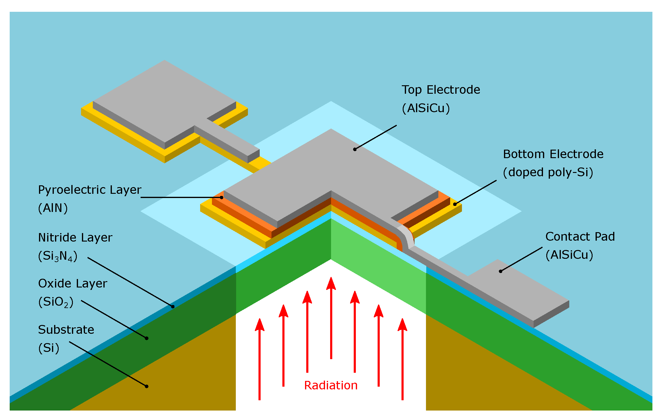
Fig. 22. Quarter cut schematic representation of the pyroelectric detector (after [38]).
Compared with AlN-based pyroelectric detectors, ScAlN-based detectors have achieved better detectivity. For 12% doped ScAlN-detector, the measured D* is above 107 cmHz1/2/W compared to 105 –106 cmHz1/2/W for AlN-based pyroelectric detectors [39]. This is explained by the higher pyroelectric coefficient of ScAlN.
As shown in Table 2, pure CMOS-compatible materials, such as AlN, HfO2, and ZnO, still pose a challenge for improving their performance to replace conventional pyroelectric materials.
7. Figure of merit (FOM) of uncooled IR detectors
Figure 23 compares detectivity as a function of the response time constant, τth, for various types of uncooled IR detectors, including pyroelectric, resistive bolometer, thermoelectric, and thermomechanical detectors. Experimental data are selected from the best performing ones − [36, 39−50]. In addition, two solid lines indicate thermopiles and bolometers. According to Dillner et al. [48], bolometers and thermopiles show differences in their dependence of the specific detectivity on the time constant:


where k2 = 1.67 · 108 m/Ws and k3 = 1.53 · 108 m/Ws3/2. These FOMs were introduced based on the analysis of many published experimental data concerning state-of-theart thermopiles and bolometers operated at room temperature.
As shown in Fig. 23, the most sensitive roomtemperature IR detector, made via a low-cost process with a speed comparable to that of commercial detectors, is a nano-optomechanical silicon nitride resonator with a thinfilm platinum absorber and 47% average broadband absorption [46]. This nanomechanical resonator consists of 50 nm silicon nitride membranes deposited by lowpressure chemical vapour deposition (LPCVD), with several thousand microns in side length. Next, a thin layer of Pt with a target thickness of 5 nm was deposited using e- beam physical vapour deposition. A circular clearance was created using the lift-off process. In the final stage, the membrane was released from the rear side via KOH wet etching. To protect the metal layer during wet etching, a wafer holder was used that exposed only the rear side of the wafer.
A similar performance to that presented in [46] is observed for the DTGS pyroelectric detector [41] and the Ti-SiNx-Ni perforated subwavelength absorber [45]. This second detector is characterised by an absorption-per-unitthermal mass-per-area of 1.5 · 1022 kg-1 m-2, which is approximately 1.6–32.1 times greater than the state-of-theart absorbers reported for any infrared application.
Results presented in Fig. 23 for CMOS-compatible pyroelectric uncooled thermal detectors are promising but still indicate a challenge in improving their performance.
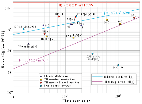
Fig. 23. Comparison of detectivity as a function of thermal time constant for uncooled IR detectors. The most sensitive IR detector operating at room temperature (manufactured using a low-cost production process), with a speed similar to standard commercial detectors, is a nano optomechanical silicon nitride resonator featuring an impedance-matched thin-film platinum absorber in free space and exhibiting an average broadband absorption of 47% [46].
8. Conclusions
Over the past two decades, a new generation of uncooled IR detectors has emerged. In particular, LDS materials, with thicknesses of the order of an atom, exhibit ultra-low thermal capacity and tunable thermoelectric properties. Furthermore, integrating LDS materials with metasurfaces enables the use of periodic configurations with lengths shorter than a wavelength and local electromagnetic field amplification. This not only overcomes the limitations of low light-absorption efficiency in thermal detectors based on LDS materials, but also enables Stokes polarisation detection, thereby enabling multidimensional light-field detection. Therefore, the fundamental properties of LDS thermal detectors enable them to circumvent the performance limitations of conventional detectors.
To overcome the existing limitations of uncooled detectors, alternative thermal detection mechanisms have been explored. One of the most promising approaches is thermal IR detection with a temperature-sensitive nanomechanical resonator. Experimental results place this type of detector among the most sensitive room-temperature IR detectors reported to date [46]. Its detectivity achieves the expected theoretical performance, albeit below the fundamental limit (1.4 · 1010 cmHz1/2/W). It is expected that trampoline resonators hold the potential to reach the fundamental sensitivity threshold. On the current level of technology, nonomechanical resonators are used in singlepoint detection applications. Expanding the technology to detector arrays presents significant difficulties. Currently, nanoelectromechanical system (NEMS) resonators are used in various applications, ranging from IR spectroscopy [44] to IR [49] and terahertz radiation [27] detection.
Recently, efforts have been made to develop CMOSbased pyroelectric detector technology. The results presented in this paper are interesting, but they fall short of the performance of standard detectors that currently dominate the market. This technology still indicates a challenge in improving their performance to replace conventional pyroelectric materials.
The performance of other detectors considered in this study, such as thermoelectric and nanotube microbolometers, is inferior to that of standard detectors on the global market. One of the fundamental problems is the difficulty in increasing quantum efficiency. A widely used strategy is to exploit the optical properties of metamaterials, such as plasmonic antennas with nearly 100% absorptance or photonic crystals. However, in the last case, the devices are limited to a narrow spectral range and are expensive to fabricate.
References
[1] Kingston, R. H. Detection of Optical and Infrared Radiation. (Wiley, New York, 1983).
[2] Dereniak, E. L. & Boremen, G. D. Infrared Detectors and Systems. (Wiley, New York, 1996).
[3] Rieke, G. H. Detection of Light: From Ultraviolet to the Submillimeter. (Cambridge University Press, Cambridge, 2003).
[4] Vincent. J. D., Hodges, S. E., Vampola, J., Stegall, M. & Pierce, G. Fundamentals of Infrared and Visible Detector Operation and Testing. (Wiley, Hoboken, 2016).
[5] Donati, S. Photodetectors. Devices, Circuits, and Applications, 2[nd] ed. (Wiley, Hoboken, 2021).
[6] Rogalski, A. & Bielecki, Z. Detection of Optical Signals. (CRC Press, Boca Raton, 2022).
[7] Ludwig, F. et al. Terahertz detection with graphene FETs: Photothermoelectric and resistive self-mixing contributions to the detector response. ACS Appl. Electron. Mater. 6, 2197−2212 (2024). https://doi.org/10.1021/acsaelm.3c01511
[8] Mott, N. & Jones, H. The Theory of the Properties of Metals and Alloys. (The Clarendon Press, 1936).
[9] Nourbakhsh, A. et al. Heterogeneous Integration of 2D Materials and Devices on a Si Platform. in Beyond-CMOS Technologies for Next Generation Computer Design (Topaloglu, E. O. & Wong, H.S. P.) 43-84 (Springer International Publishing, 2019). https://doi.org/10.1007/978-3-319-90385-9_3
[10] Xia, F., Yan, H. & Avouris, P. The Interaction of Light and Graphene: Basics, Devices, and Applications. Proc. IEEE, 101, 1717–1731, (2013). https://doi.org/10.1109/JPROC.2013.2250892
[11] Wredh, S. et al. Sb2Te3–Bi2Te3 direct photothermoelectric midinfrared detection. Adv. Optical Mater. 12, 2401450 (2024). https://doi.org/10.1002/adom.202401450
[12] Greenaway, D. L. & Harbeke, G. Band structure of bismuth telluride, bismuth selenide and their respective alloys. J. Phys. Chem. Solids 26, 1585 − 1604 (1965). https://doi.org/10.1016/0022-3697(65)90092-2
[13] Tang, H., Li, Z., Liu, W., Zhang, Q. & Uher, C. A comprehensive review on Bi2Te3-based thin films: Thermoelectrics and beyond. Interdiscip. Mater. 1, 88 − 115 (2022). https://doi.org/10.1002/idm2.12009
[14] Yang, S. et al. Enhanced evanescent field coupling of smart particles in tubular optical microcavity for sensing application. Adv. Opt. Mater. 10, 2102158 (2021). https://doi.org/10.1002/adom.202102158
[15] Huang, J. et al. Enhanced photothermoelectric conversion in selfrolled tellurium photodetector with geometry-induced energy localization. Light Sci. Appl. 13, 153 (2024). https://doi.org/10.1038/s41377-024-01496-0
[16] Varpula, A. et al. Thermoelectric thermal detectors based on ultrathin heavily doped single-crystal silicon membranes. Appl. Phys. Lett. 110, 262101 (2017). https://doi.org/10.1063/1.4989683
[17] Varpula, A. et al. Nano-thermoelectric infrared bolometers. APL Photon. 6, 036111 (2021). https://doi.org/10.1063/5.0040534
[18] Varpula, A. et al. High-performance infrared thermoelectric bolometers based on nanomembranes. Proc. SPIE 11289, 112891O (2020). https://doi.org/10.1117/12.2542194
[19] Varpula, A . et al. Uncooled nano-thermoelectric bolometers for infrared imaging and sensing. Proc. SPIE 12417, 124170U (2023). https://doi.org/10.1117/12.2646314
[20] Cary, H. H. Infrared radiation detector employing tensioned foil to receive radiation. U.S. Patent US3 457 412A, vol. 7, 1969.
[21] Larsen, T. et al. Ultrasensitive string-based temperature sensors. Appl. Phys. Lett. 98, 121901 (2011). https://doi.org/10.1063/1.3567012
[22] Yamada, S., Schmid, S., Larsen, T., Hansen, O. & Boisen A. Photothermal infrared spectroscopy of airborne samples with mechanical string resonators. Anal. Chem. 85, 10531–10535 (2013). https://doi.org/10.1021/ac402585e
[23] Larsen, T., Schmid, S. & Boisen, A. Micro string resonators as temperature sensors. AIP Conf. Proc. 1552, 931–936 (2013). https://doi.org/10.1063/1.4819669
[24] Qian, Z., Rajaram, V., Kang, S. & Rinaldi, M. High figure-of-merit NEMS thermal detectors based on 50-nm thick AlN nano-plate resonators. Appl. Phys. Lett. 115, 261102 (2019). https://doi.org/10.1063/1.5128643
[25] Piller, M., Luhmann, N., Chien, M.-H. & Schmid, S. Nanoelectromechanical infrared detector. Proc. SPIE 11088, 1108802 (2019). https://doi.org/10.1117/12.2528416
[26] Piller, M. et al. Thermal IR detection with nanoelectromechanical silicon nitride trampoline resonators. IEEE Sens. J. 23, 1066–1071 (2023). https://doi.org/10.1109/JSEN.2022.3223439
[27] Vicarelli, L., Tredicucci, A. & Pitanti, A. Micromechanical bolometers for subterahertz detection at room temperature. ACS Photonics 9, 360–367 (2022). https://doi.org/10.1021/acsphotonics.1c01273
[28] Blaikie, A., Miller, D. & Alemán, B. J. A fast and sensitive roomtemperature graphene nanomechanical bolometer. Nat. Commun. 10, 4726 (2019). https://doi.org/10.1038/s41467-019-12562-2
[29] Duraffourg, L., Laurent, L., Moulet, J.-S., Arcamone, J. & Yon, J.J. Array of resonant electromechanical nanosystems: A technological breakthrough for uncooled infrared imaging. Micromachines 9, 401 (2018). https://doi.org/10.3390/mi9080401
[30] Laurent, L., Yon, J.-J., Moulet, J.-S., Roukes, M. & Duraffourg, L. 12- μ m-pitch electromechanical resonator for thermal sensing. Phys. Rev. Appl. 9, 024016 (2018). https://doi.org/10.1103/PhysRevApplied.9.024016
[31] Rogalski, A. Infrared and Terahertz Detectors. (CRC Press, Boca Raton, 2019).
[32] Yadav, P.V.K. et al. Advancements of uncooled infrared microbolometer materials: A review. Sens. Actuators A: Phys. 342, 113611 (2022). https://doi.org/10.1016/j.sna.2022.113611
[33] Nandi, S. & Misra, A. Carbon nanotube-based uncooled bolometers: Advances and progress. ACS Mater. Lett. 5, 249−274 (2023). https://doi.org/10.1021/acsmaterialslett.2c00680
[34] Michel, M. et al. Scalable nanotube-microbolometer technology with pixel pitches from 12 down to 6 µm. Proc. SPIE 11537, 1153704 (2020). https://doi.org/10.1117/12.2573895
[35] Michel, M., Blaeser, S., Zakizade, E., Weyers, S. & Weiler, D. 6 µm microbolometers for uncooled thermal imaging. Proc. SPIE 11866, 1186605 (2021). https://doi.org/10.1117/12.2597969
[36] Wu, B. et al. One-step rolling fabrication of VO2 tubular bolometers with polarization-sensitive and omnidirectional detection. Sci. Adv. 9, eadi7805 (2023). https://doi.org/10.1126/sciadv.adi7805
[37] Ranu, Uthra, B., Sinha, S. & Agarwal, B. P. CMOS compatible pyroelectric materials for infrared detectors. Mater. Sci. Semicond. Process 140, 106375 (2022). https://doi.org/10.1016/j.mssp.2021.106375
[38] Ranacher, C. et al. A CMOS compatible pyroelectric mid-infrared detector based on aluminium nitride. Sensors 19, 2513 (2019). https://doi.org/10.3390/s19112513
[39] Ng, D. K. T. et al. A functional CMOS compatible MEMS pyroelectric detector using 12%-doped scandium aluminum nitride. Appl. Phys. Lett. 117, 183506 (2020). https://doi.org/10.1063/5.0024192
[40] Lehmkau, R. et al. Fully CMOS-compatible pyroelectric infrared detector based on doped HfO2 thin film in 3D-integration. Proc. SPIE 12002, 120020M (2022). https://doi.org/10.1117/12.2607271
[41] D31/L31/LT31 Series. Single Channel Voltage Mode Pyroelectric Detectors Laser Components https://www.lasercomponents.com/fileadmin/user_upload/home/Da tasheets/lc-pyros/d31-lt31-vm-pyro-detectors.pdf
[42] Schnelle, W., Dillner, U., Scheike, B. & Albrecht, L. Infrared Radiation Sensors Based on Thin Film Bolometers. in Proc. of the 2nd Symposium on Temperature Measurement in Industry and Science 16–18 (1984).
[43] Foote, M. C. et al. Thermopile Detector Arrays for Space Science Applications. in International Thermal Detectors Workshop (TDW 2003) 2–26 (2004).
[44] Piller, M. et al. Thermal IR detection with nanoelectromechanical silicon nitride trampoline resonators. IEEE Sens. J. 23, 1066–1071 (2023). https://doi.org/10.1109/JSEN.2022.3223439
[45] Das, A., Mah, M. L., Hunt, J. & Talghader, J J. Thermodynamically limited uncooled infrared detector using an ultra-low mass perforated subwavelength absorber. Optica 10, 1018–1028 (2023). https://doi.org/10.1364/OPTICA.489761
[46] Martini, P. et al. Uncooled thermal infrared detection near the fundamental limit using a silicon nitride nanomechanical resonator with a broadband absorber. Commun. Phys. 8, 166 (2025). https://doi.org/10.1038/s42005-025-02093-2
[47] Dong, L., Yue, R.-F. & Liu, L.-T. An uncooled microbolometer infrared detector based on polycrystalline silicon germanium thin film. Int. J. Nonlinear Sci. Numer. Simul. 3, 303–306 (2002). https://doi.org/10.1016/S0924-4247(03)00232-2
[48] Dillner, U., Kessler, E. & Meyer, H.-G. Figures of merit of thermoelectric and bolometric thermal radiation sensors J. Sens. Sens. Syst. 2, 85–94 (2013). https://doi.org/10.5194/jsss-2-85-2013
[49] Zhang, C. et al. High detectivity terahertz radiation sensing using frequency-noise-optimized nanomechanical resonators. APL Photonics 9, 126105 (2024). https://doi.org/10.1063/5.0238977
[50] Lei, C. et al. A double-end-beam based infrared device fabricated using CMOS-MEMS process. Sens. Rev. 36, 240–248 (2016). https://doi.org/10.1108/SR-02-2016-0038