Nb2O5-doped TiO2 film synthesised via sol-gel method – technology and optical characterisation
Magdalena Zięba1 *
Cuma Tyszkiewicz1
Zbigniew Opilski1
Kamil Barczak1
Jacek Nizioł2
Ewa Gondek3
Paweł Karasiński1
- Department of Optoelectronics, Silesian University of Technology, ul. Bolesława Krzywoustego 2, 44-100 Gliwice, Poland
- Faculty of Physics and Applied Computer Science, AGH University of Krakow, Al. Adama Mickiewicza 30, 30-059 Kraków
- Institute of Physics, Cracow University of Technology, ul. Podchorążych 1, 30-084 Kraków, Poland
Article Info
Received 27 Oct. 2025
Received in revised form 13 Jan. 2026
Accepted 18 Feb. 2026
Available on-line 21 Apr. 2026
Keywords: titanium film; niobium; sol-gel; dip-coating.
Abstract
This study reports the results of an investigation of a niobium-doped titania dioxide thin film fabricated via a sol-gel method and dip-coating. Niobium-doped and undoped titania films were deposited on silicon wafers and soda-lime glass slides. The niobium-doped and undoped titanium dioxide films exhibit a high refractive index of ∼ 2.1 and thicknesses exceeding 110 nm. The study addresses the technological procedures, characterisation methods, and the influence of niobium doping on the optical properties of TiO2 films.
1. Introduction
Thin layers of titanium dioxide (TiO2) have enormous application potential because of their chemical and biological neutrality and excellent physical and chemical stability. In addition, TiO2 exhibits a high refractive index and excellent transparency in the VIS-NIR spectral range. The optical and electrical properties of TiO2 films are closely related to their structural characteristics, which can be intentionally tailored during the fabrication processes [1–6]. For these reasons, TiO2 has long been the focus of many research groups [7–10].
TiO2 thin films may be either amorphous or polycrystalline in the form of anatase or rutile, which are both tetragonal. Polycrystalline films fabricated at low temperatures (below 600 °C) contain only the anatase phase, which is explained by anatase lower surface energy compared to rutile [10–11]. Anatase is a wide-bandgap, n type semiconductor. It has a relatively large indirect bandgap (3.2 eV in bulk) and a high refractive index (n ~ 2.5). As a result of the quantum size effect, TiO2 nanocrystals exhibit a wider optical bandgap than bulk crystals [12–14].
However, due to porosity, the refractive indices of TiO2 thin films (amorphous and polycrystalline) are often lower than those of anatase single crystals [14, 15].
Doping with niobium (Nb) in the form of Nb2O5 improves the stability of TiO2 at the nanoscale [10]. Nb2O3-doped TiO2 (Nb:TiO2) is considered a prospective material from the point of view of transparent conductive oxide (TCO) fabrication technology and its applications. This is because it has an excellent optical transparency, a high refractive index and high electrical conductivity. Nb2O5 has a wide bandgap of 3.4–3.6 eV and a high refractive index of 2.2–2.6. Nb:TiO2 thin films have been synthesised using various methods, including magnetron sputtering [16, 17], atomic layer deposition (ALD) [18, 19], chemical vapour deposition (CVD) [20], and the sol-gel method [21–23].
The subject of the reported work is niobium-doped TiO2 films fabricated by the sol-gel method and dip-coating technique. The sol-gel method offers several advantages, including precise control of material structure over a wide range, low-temperature processing, ability to produce multicomponent materials with molecular-level homogeneity, and flexibility to modify physicochemical properties through doping. The aim of this work is to present the results of investigations on the effect of niobium doping on the optical properties of TiO2 films. In this paper, we present the impact of a substrate withdrawal speed from the sol on the final thicknesses and refractive indices of Nb:TiO2 films, the effect of film thickness on the optical bandgap, the dispersion characteristics of the refractive index and the extinction coefficient, and the effect of film thickness on the optical bandgap. In each case, results obtained for the reference TiO2 films are also presented for comparison.
2. Synthesis and characterisation
2.1. Materials
Titanium (IV) ethoxide (TET, technical grade, SigmaAldrich, Steinheim, Germany) was selected as a precursor for titania dioxide. Niobium(V) ethoxide (99.95%, SigmaAldrich, Steinheim, Germany) served as the niobium oxide source. Polyethylene glycol (PEG-300, Mn = 300, SigmaAldrich, Steinheim, Germany) was employed as a surfactant. Absolute ethanol (EtOH; 99.8%, AR grade) and hydrochloric acid (HCl; 36%, AR grade) were obtained from Avantor Performance Materials (Gliwice, Poland). Soda-lime microscope slides (Menzel Gläser, Thermo Scientific, n = 1.513 at λ = 632.8 nm) of a dimension of 76 × 26 ×1 mm3 and silicon wafers were used as substrates. The sol solutions were filtered using Whatman Puradisc PTFE syringe filters (25 mm diameter, 0.2 µm pore size, Sigma-Aldrich).
2.2. Preparation of sol and film fabrication
The sol for reference TiO2 films was synthesised using our procedure reported earlier in [15]. The niobium oxidedoped titania sol was prepared using a modified version of the method described in [15]. A total of 0.14 moles of the titanium (IV) ethoxide and 0.016 moles of niobium (V) ethoxide were added to 0.99 moles of absolute ethanol and 0.22 moles of deionised water. Subsequently, 0.02 moles of PEG-300 and 0.06 moles of HCl were added to the reaction mixture under ambient conditions to initiate hydrolysis and condensation. The synthesis was carried out under ultrasound for 2.5 h at 50 °C. The sol was filtered through a syringe membrane and subsequently aged for 24 h. Nb:doped-TiO2 and undoped TiO2 films were fabricated on soda-lime glass and silicon wafers using the dip-coating technique. The range of withdrawal speeds used was 3 ÷ 7 cm/min. The films were then annealed for 60 minutes at 500 ° C .
2.3. Methods
The film thickness d and refractive index n were determined using a SENTECH SE400 monochromatic ellipsometer operating at a wavelength of λ = 632.8 nm (SENTECH Instruments GmbH, Germany). All other ellipsometric measurements were performed using a spectroscopic ellipsometer M-2000D from J. A. Wollam, which acquires data at 709 wavelengths in the spectral range from 1690 nm to 193 nm (0.73 eV to 6.52 eV). The probing light, with a beam diameter of approximately 3 mm, was incident on the sample surface at angles near the Brewster angle, specifically 60°, 65°, and 70°. The measurements were conducted at the sample centre and at a 5 mm-spaced square grid consisting of 9 points.
The transmittance and reflectance of the fabricated films were investigated using a UV-VIS AvaSpec-ULS2048LTEC spectrophotometer (Avantes, Apeldoorn, The Netherlands). At room temperature, the transmittance and reflectance were measured using an AvaLight-DH-S-BAL (Avantes) light source over the spectral range of 300–1000 nm.
3. Results and discussion
In the dip-coating technique, the film thickness is primarily controlled by the substrate withdrawal speed v [24]. The effect of substrate withdrawal speed v on the film thickness (d) and refractive index (n) of the TiO2 and Nb:TiO2 films is shown in Fig. 1. Blue diamond markers represent experimental data for the reference TiO2 films, whereas red diamond markers correspond to Nb:TiO2 films. Solid diamond markers indicate the experimental characteristics d = d(v), while hollow diamond markers indicate n = n(v). The films thicknesses increase with the withdrawal speed of the substrates from the sols while the refractive indices remain constant, equal to n = 2.074 ± 0.001 for undoped TiO2 films and n = 2.110 ± 0.002 for Nb:TiO2 films. As shown in Fig. 1, for all v, the Nb:TiO2 films are thicker than the undoped TiO2 films. This is due to the increased viscosity of the sol from which the films were deposited. By changing the withdrawal speed of the substrates from sols from 3.2 cm/min to 6.6 cm/min, films with thicknesses from ca. 120 nm to ca. 180 nm were produced, with the thickness of the Nb:TiO2 film being ca. 5 nm greater for each withdrawal speed.
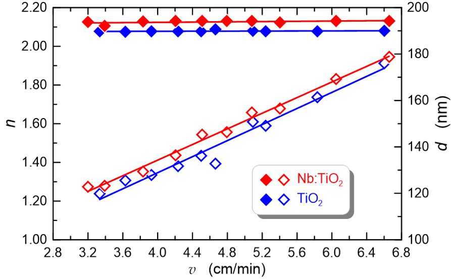
Fig. 1. Dependence of thickness d and refractive index n on the substrate withdrawal speed for the Nb:TiO2 and TiO2 films. All films were annealed at 500 °C for 1 h, λ = 632.8 nm.
The refractive indices of the produced films are lower than that of anatase (nd = 2.52), indicating that the films are porous. The porosity P of the films was determined using the Lorentz-Lorenz equations:

assuming the pores are filled with air. It was calculated that undoped TiO2 films have a porosity of 18%, while Nb:TiO2 films have a slightly lower porosity of 15%, indicating that the Nb:TiO2 films are more compact than undoped TiO2 films.
An image of exemplary Nb:TiO2 and TiO2 films on a soda-lime glass slide is shown in Fig. 2. The photograph was taken in sunlight. Uniform interference colours can be observed across the entire surface, indicating uniformity in both the refractive index and the film thickness. All prepared films were free of cracks and showed uniformity and continuity.
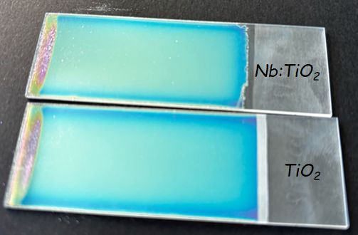
Fig. 2. Images of selected Nb:TiO2 and TiO2 films deposited on soda-lime glass slides. In both cases, the withdrawal speed of the substrates from the sols was the same: v = 6 cm/min.
The optical homogeneity of the films was verified by comparing their reflectance spectra with those of the sodalime glass substrates, as shown in Fig. 3. The reflectance spectra of the tested structures exhibit distinct interference minima and maxima. As shown, for wavelengths greater than 350 nm, both interference minima of the doped film coincide with the reflectance spectrum of the glass substrates used. This is clear evidence of the film optical homogeneity [25]. For the reference film at a wavelength of ∼ 380 nm, the interference minimum is slightly above the substrate reflectance due to the absorption edge.
The transmittance spectra for the same structures are shown in Fig. 4. In both cases, a strong decay of transmittance is visible for wavelength λ = 382 nm (hν = 3.25 eV), which results from the presence of an absorption edge. For wavelength λ < 310 nm (hν > 4.0 eV), the transmittance disappears completely. The Tauc method was applied to the transmittance spectra to determine the optical bandgaps in this spectral range [14, 26].
Figure 5 shows the exemplary plot of (α · hν)1/2 and (α · hν)2 on the energy photon for Nb:TiO2 (d = 169 nm) film deposited on a glass substrate of the same kind. To determine the optical bandgap, a straight-line segment of the normalised absorption vs. photon-energy graph is used. This segment is approximated by a linear relationship, extrapolated to its intersection with the horizontal axis (hν). The photon energy at the intersection point equals the optical bandgap Eg. The determined values of the indirect and direct energy bandgaps were 3.45 eV and 3.75 eV, respectively.
The influence of the film thickness (d) on values of optical bandgaps (Eg) for direct and indirect transitions is presented in Fig. 6. Full circles and diamonds mark the energy bandgaps for indirect optical transitions, while empty circles and diamonds correspond to direct optical transitions. In each case, the experimental dependences were approximated by linear functions. The relationships for niobium-doped films (Nb:TiO2) are plotted in red and for undoped films (TiO2) in blue. All graphs show slight decreases in the energy bandgap with increasing film thickness, a typical effect in thin films.
As can be clearly seen, the energy bandgap of niobiumdoped films is larger than that of undoped films over the
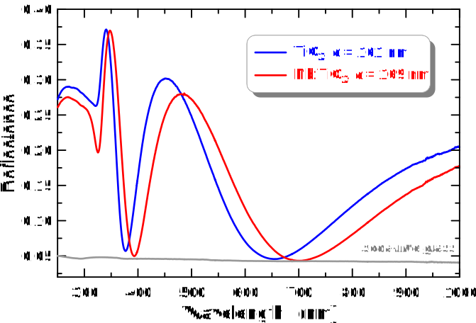
Fig. 3. Reflectance spectra of selected Nb:TiO2 and TiO2 films on soda-lime glass slides.
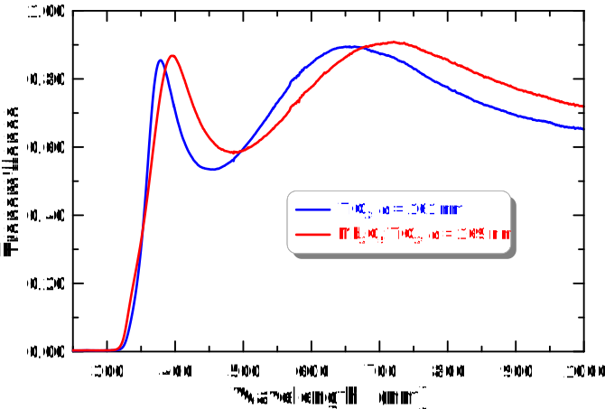
Fig. 4. Transmittance spectra of selected Nb:TiO2 and TiO2 films on soda-lime glass slides.
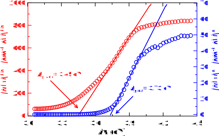
Fig. 5. Normalised absorption coefficients vs. photon energy for Nb:TiO2 films, d = 169 nm.
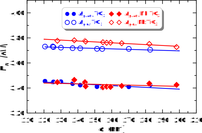
Fig. 6. The influence of film thickness on the energy bandgaps.
entire thickness range. However, for indirect optical transitions, there are no significant differences between the optical bandgaps for doped and undoped films. The indirect optical bandgap for Nb:TiO2 is in the range of 3.42 eV to 3.45 eV. These energies are higher than the optical bandgap of anatase, which is equal to 3.2 eV (bulk crystal). This blue-shifted energy bandgap is a quantum-size effect. Based on the magnitude of this shift, the diameters of anatase nanocrystals were estimated to be ca. 4 nm, as described in our earlier works [14, 15]. In [15, 24], we showed that the diameters of anatase nanocrystals determined in this way are comparable to the diameters determined from TEM images.
The spectral dispersion characteristics of the ellipsometric angles Ψ and Δ were recorded over wavelengths from 200 to 1700 nm, for selected sample illumination angles of 60 °, 70 °, and 75 °. The characteristics Ψ(λ) and Δ(λ) recorded for the Nb:TiO2 on silicon substrate are presented in Figs. 7 and 8, respectively. A two-stage approach was used to develop the results. In the first stage, the upper wavelength limit for fits was set at 400 nm, corresponding to an energy of 3.1 eV. The choice can be easily justified based on Figs. 7 and 8. For energies higher than ca. 3.1 eV, the observed beats change their form, an effect occurring due to light absorption. The second limit was set at 270 nm (4.6 eV). For shorter wavelengths,
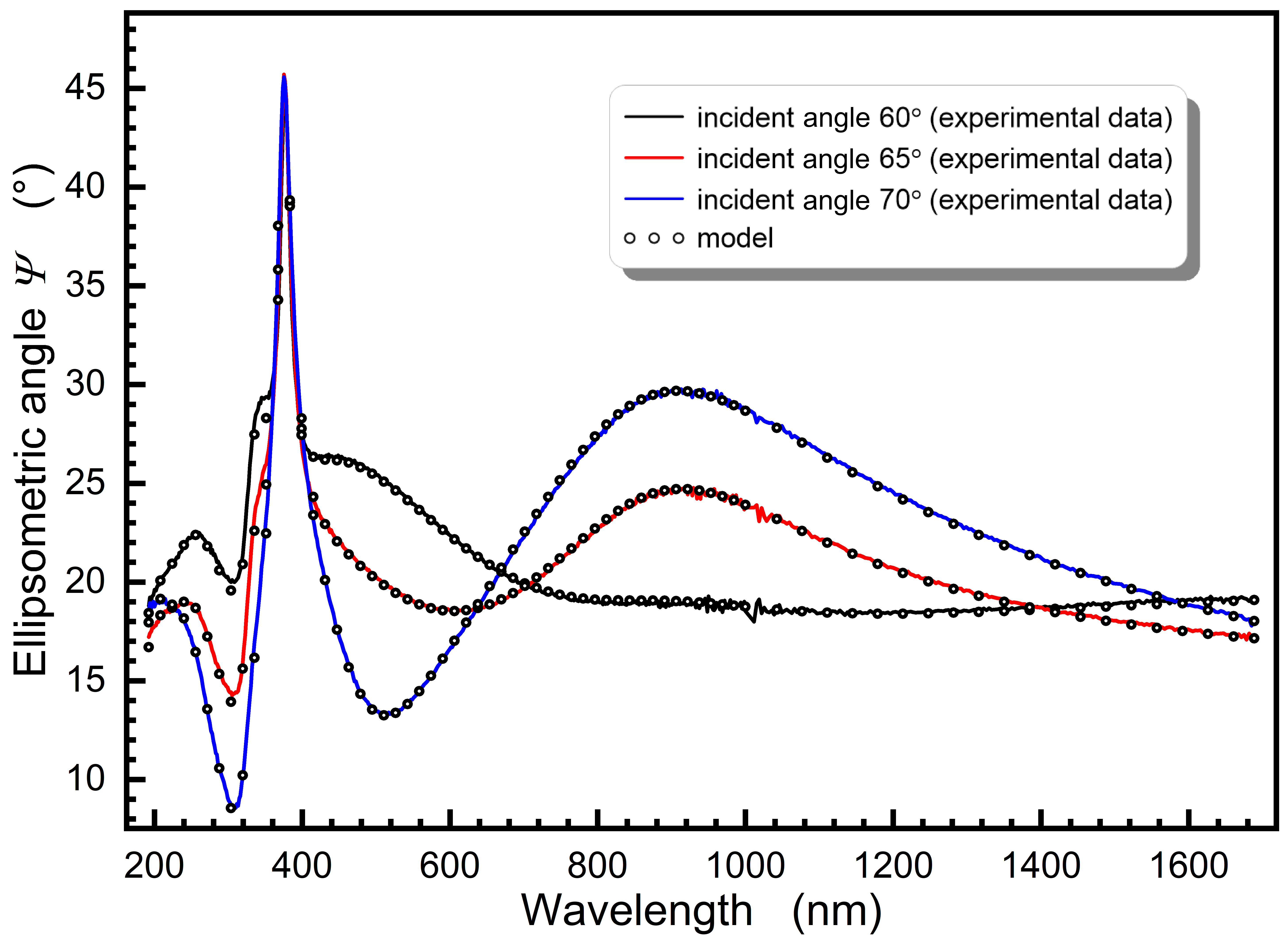
Fig. 7. Example of the dependence of the ellipsometric angle Ψ on the wavelength of the incident light, for the angle of incidence equal to 60°, 65°, and 70°. Data were collected for the sample manufactured from Nb:TiO2. Black dots correspond to the fitted B-spline model.
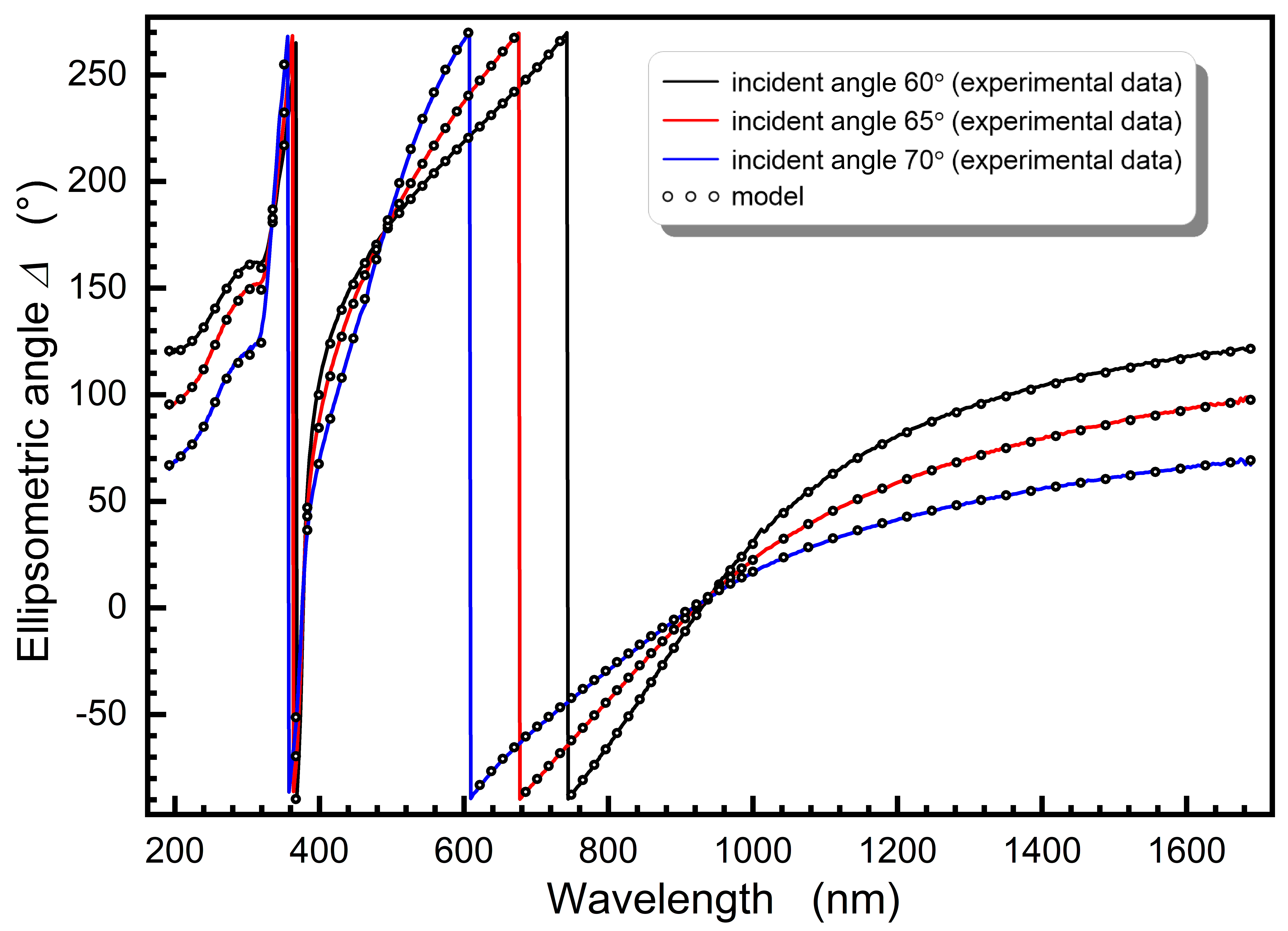
Fig. 8. Example of the dependence of the ellipsometric angle Δ on the wavelength of the incident light and the incidence angle (60°,65°,70°). Data were collected for the sample, which consisted of undoped Nb:TiO2. Black dots correspond to the fitted B-spline model.
beats disappear entirely, indicating that the incident light is completely absorbed in the material and reflected only at the upper surface of the film. The latter renders the analysis flawed due to the assumptions underlying the models used to fit the ellipsometric data. At first, the sample thickness was calculated using the Sellmeier approximation, which is valid in the transparent spectral region and is often used to model the optical constants of transparent dielectric materials. The Sellmeier approximation allowed us to determine the film thickness at each test point, while other parameters were kept constant across all points. The results were averaged across the tested samples. Next, using the above results, the entire spectrum (up to 270 nm) was fitted with B-spline polynomials, imposing Kramers–Kronig order, and a positive imaginary part of the dielectric constant. The fit quality was assessed by minimising the mean-squared error between the measured and modelgenerated parameters across all measurement wavelengths. Finally, the results were averaged. Spectral dispersion characteristics of the real n (λ) and imaginary κ (λ) part of the refractive index, determined in this way for the Nb:TiO2 films and the pure TiO2 films on silicon substrates, respectively, are shown in Figs. 9 and 10. As shown, over the entire spectral range, the refractive index of the Nb:TiO2 film is higher than that of the undoped film. This means that niobium-doped titania films are more compact than undoped films. However, the extinction coefficients of both films are zero for wavelengths > 400 nm and attain significant values only below 400 nm. For this reason,
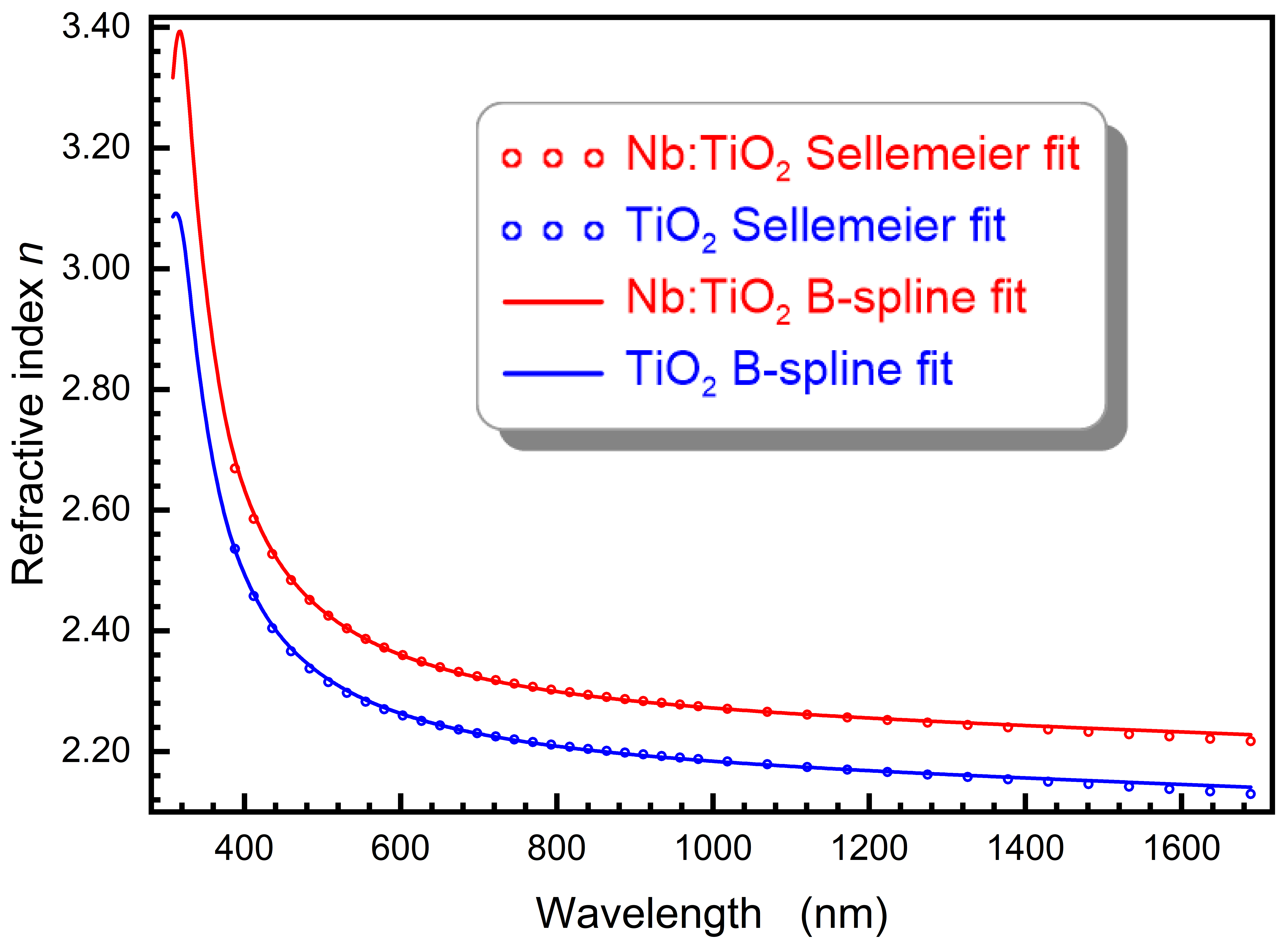
Fig. 9. Dispersion of refractive index found for the samples studied.
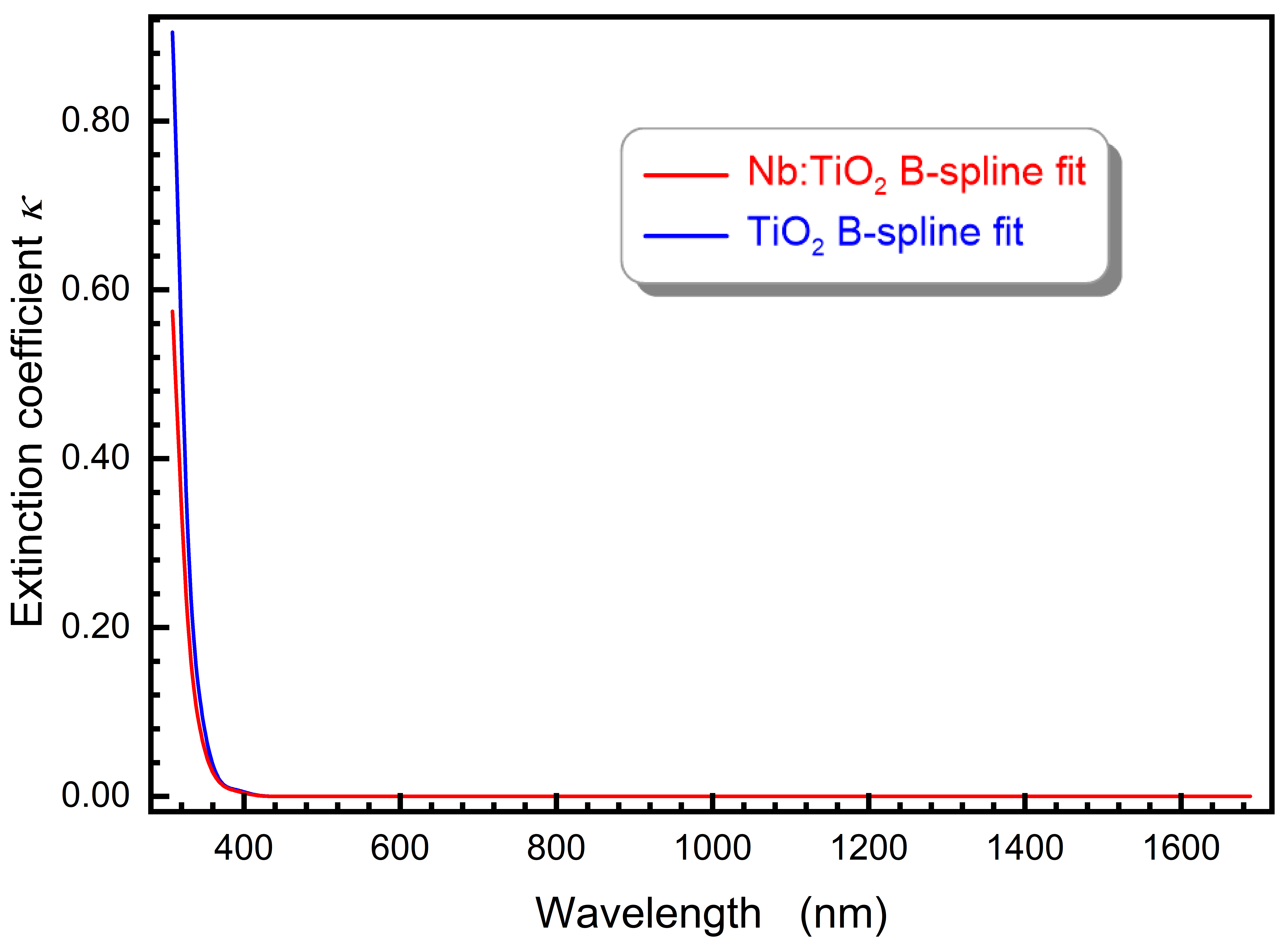
Fig. 10. Dispersion of extinction coefficient found for the samples studied.
the minima of the reflectance spectra shown in Fig. 3 in the spectral range below 400 nm are not associated with the substrate reflectance characteristics.
The refractive indices of Nb:TiO2 and TiO2 films on silicon substrates are approximately 0.15 higher than the refractive indices of the same films on soda-lime glass substrates (Fig. 1). The lower refractive indices of the films on soda-lime glass substrates are the result of sodium ion diffusion from the substrate into the film, which promotes TiO2 crystallisation, i.e., the formation of a more differentiated, more porous film structure [27].
4. Conclusions
Optically uniform niobium oxide-doped and undoped TiO2 films have been deposited on soda-lime glass substrates and silicon wafers using the sol-gel method and dip-coating technique. The results of the study presented here on the effect of niobium doping on the optical properties of these films demonstrated the impact of doping on sol viscosity. As a result, doped and undoped films produced at the same withdrawal speeds differ in thickness. Spectrophotometric measurements confirmed the optical homogeneity of both niobium-doped and undoped TiO2 films.
Authors’ statement
Conceptualisation, investigation, formal analysis, writing – original draft, writing – review and editing, visualisation, M.Z.; investigation, software, formal analysis, writing – original draft, writing – review and editing, visualisation; supervision, funding acquisition, C.T.; investigation, formal analysis, validation, Z.O.; investigation, formal analysis, K.B.; investigation, formal analysis, validation; writing – original draft, J.N.; investigation, formal analysis, validation, E.G.; conceptualisation, formal analysis, writing – original draft, writing – review and editing, visualisation, supervision, P.K.
Acknowledgements
This publication has been co-financed from the state budget under the Ministry of Education and Science’s ”Polish Metrology II” programme (project no. PM‑II/SP/0042/ 2024/02); the amount of co-financing is PLN 1 000 000 and the total value of the project is PLN 1 000 000.
Additional support was provided by the Faculty of Electrical Engineering at the Silesian University of Technology via grant BKM‑533/RE4/2025.

References
[1] Jolivet, A. et al. Structural, optical, and electrical properties of TiO2 thin films deposited by ALD: Impact of the substrate, the deposited thickness and the deposition temperaturę. Appl. Surf. Sci. 608, 155214 (2023). https://doi.org/10.1016/j.apsusc.2022.155214
[2] Bange, K. et al. Investigations of TiO2 films deposited by different techniques. Thin Solid Films 197, 279–285 (1991). https://doi.org/10.1016/0040-6090(91)90238-S
[3] Ottermann, C. R. & Bange, K. Correlation between the density of TiO2 films and their properties. Thin Solid Films 286, 32–34 (1996). https://doi.org/10.1016/S0040-6090(96)08848-7
[4] Huong, N. T. M., Binh, N. T., Huong, L. T. T., Dung, N. D. & Tinh, N. T. Effect of fabrication process on the hydrophilic properties of porous TiO2 thin films for self-cleaning application. Mater. Sci. Eng. B 6, 126–130 (2016). https://doi.org/10.17265/2161-6221/2016.5-6.002
[5] Mulus, D. A. S., Permana, M. D., Deawati, Y. & Eddy, D. R. A current review of TiO2 thin films: Synthesis and modification effect to the mechanism and photocatalytic activity. Appl. Surf. Sci. Adv. 27, 100746 (2025). https://doi.org/10.1016/j.apsadv.2025.100746
[6] Diebold, U. Structure and properties of TiO2 surfaces: A brief review. Appl. Phys. A 76, 681–687 (2003). https://doi.org/10.1007/s00339-002-2004-5
[7] Jiang, K. et al. Low-temperature, solution processing of TiO2 thin films and fabrication of multilayer dielectric optical elements. Solid State Sci. 11, 1692–1699 (2009). https://doi.org/10.1016/j.solidstatesciences.2009.05.026
[8] Płacheta, K. et al. Evolution of surface properties of titanium oxide thin films. Appl. Surf. Sci. 608, 155046 (2023). https://doi.org/10.1016/j.apsusc.2022.155046
[9] Kania, A., Pilarczyk, W. & Szindler, M. M. Structure and corrosion behavior of TiO2 thin films deposited onto Mg-base alloy using magnetron sputtering and sol-gel . Thin Solid Films 701, 137945 (2020). https://doi.org/10.1016/j.tsf.2020.137945
[10] da Silva, A. L., Hotza, D. & Castro, R. H. R. Surface energy effects on the stability of anatase and rutile nanocrystals: A predictive diagram for Nb2O5-doped-TiO2. Appl. Surf. Sci. 393, 103–109 (2017). https://doi.org/10.1016/j.apsusc.2016.09.126
[11] Hanaor, D. A. H. & Sorrell, C. C. Review of the anatase to rutile phase transformation. J. Mater. Sci. 46, 855–874 (2011). https://doi.org/10.1007/s10853-010-5113-0
[12] Brus, L. E. Electron-electron and electron-hole interactions in small semiconductor crystallites: The size dependence of the lowest excited electronic state. J. Chem. Phys. 80, 4403–4409 (1984). https://doi.org/10.1063/1.447218
[13] Kayanuma, Y. Quantum-size effects of interacting of electrons and holes in semiconductor microcrystals with spherical shape. Phys Rev. B 38, 9797–9805 (1988). https://doi.org/10.1103/PhysRevB.38.9797
[14] Karasiński, P., Gondek, E., Drewniak, S. & Kityk, I. V. Nano-sized blue spectral shift in sol–gel derived mesoporous titania films. J. Sol-Gel Sci. Technol. 61, 355–361 (2012). https://doi.org/10.1007/s10971-011-2634-1
[15] Zięba, M. et al. Cost-effective titania layers over 100 nm thick – effect of annealing on the structural, morphological, and optical properties. Opto-Electron. Rev. 31, e147913 (2023). https://doi.org/10.24425/opelre.2023.147913
[16] Coşkun, Ö. D. & Demirela, S. The optical and structural properties of amorphous Nb2O5 thin films prepared by RF magnetron sputtering. Appl. Surf. Sci. 277, 35–39 (2013). https://doi.org/10.1016/j.apsusc.2013.03.116
[17] Dorow-Gerspach, D., Mergel, D. & Wuttig, M. Effects of different amounts of Nb doping on electrical, optical, and structural properties in sputtered TiO2x films. Crystals 11, 301 (2021). https://doi.org/10.3390/cryst11030301
[18] Niemela, J. P., Hirose, Y., Hasegawa, T. & Karppinen, M. Transition in electron scattering mechanism in atomic layer deposited Nb:TiO2 thin films. Appl. Phys. Lett. 106, 042101 (2015). https://doi.org/10.1063/1.4906865
[19] Berghuis, W. J. H. et al. Atomic layer deposition of Nb-doped TiO2: Dopant incorporation and effect of annealing. J. Vac. Sci. Technol. A 38, 022408 (2020). https://doi.org/10.1116/1.5134743
[20] Gardecka, A. J., Goh, G. K. L., Sankar, G. & Parkin, I. P. On the nature of niobium substitution in niobium doped titania thin films by AACVD and its impact on electrical and optical properties. J. Mater. Chem. A 3, 17755–17762 (2015). https://doi.org/10.1039/C5TA03772G
[21] Lu, Y. et al. Doping concentration effects upon column-structured Nb:TiO2 for transparent conductive thin films prepared by a sol–gel method. J. Alloy. Compd. 663, 413–418 (2016). https://doi.org/10.1016/j.jallcom.2015.12.102
[22] Liu, R. et al. Preparation of Nb-doped TiO2 films by sol-gel method and their dual-band electrochromic properties. Ceram. Int. 47, 31834–31842 (2021). https://doi.org/10.1016/j.ceramint.2021.08.067
[23] Gomes, G. H. M., de Jesus, M. A. M. L., Ferlauto, A. S., Viana, M. M. &·Mohallem, N. D. S. Characterization and application of niobium‑doped titanium dioxide thin films prepared by sol–gel proces. Appl. Phys. A 127, 641 (2021). https://doi.org/10.1007/s00339-021-04781-6
[24] Karasiński, P. et al. Sol-gel derived silica-titania waveguide films for applications in evanescent wave sensors – Comprehensive study. Materials 15, 7641 (2022). https://doi.org/10.3390/ma15217641
[25] Karasiński, P. et al. Homogeneity of sol-gel derived silica-titania waveguide films – spectroscopic and AFM studies Opt. Laser Technol. 121, 105840 (2020). https://doi.org/10.1016/j.optlastec.2019.105840
[26] Tauc, J. Amorphous and Semiconductors. (Plenum Press, 1974).
[27] Gondek, E., Karasiński, P. and Drewniak, S. Nano-quantum size effect in sol–gel derived mesoporous titania layers deposited on soda-lime glass substrate. Phys. E: Low-Dimens. Syst. Nanostuctures 62, 128–135 (2014). https://doi.org/10.1016/j.physe.2014.04.018